Method of measuring micro-structure, micro-structure measurement apparatus, and micro-structure analytical system

a microstructure and analytical system technology, applied in the direction of measurement devices, semiconductor/solid-state device testing/measurement, instruments, etc., can solve the problems of lowering the yield ratio, insufficient precision in the control of the lithographic process or etching process, and the measurement will never be applicable to samples which cannot be subjected to destructive inspection

Inactive Publication Date: 2005-10-06
NEC ELECTRONICS CORP
View PDF2 Cites 14 Cited by
  • Summary
  • Abstract
  • Description
  • Claims
  • Application Information

AI Technical Summary

Problems solved by technology

Insufficient precision in the control of the lithographic process or etching process may fail in obtaining a stable single-mode oscillation, fail in obtaining oscillation threshold value or optical output satisfactory in view of product standards, or result in a lowered yield ratio.
Measurement under a scanning electron microscope, however, raises a problem in that observation of the sectional shape inevitably needs cutting of the sample, so that the measurement will never be applicable to the samples which cannot be subjected to destructive inspection.
On the other hand, non-destructive observation of the surface state under a CD-SEM raises difficulty in measurement of correct shape, because depth-wise information cannot be obtained.
Another problem of the measurement under the electron microscope resides in that it takes a long time due to need of setting of the sample in vacuo, so that the measurement is not fully applicable to the mass production process.
The methods of measuring line width of a periodic structure described in Japanese Laid-Open Patent Publication No. 11-211421 and ditto No. 2001-217291, however, raise a problem in that only a limited amount of reflection characteristic data is measurable, and in that information on the height cannot be obtained, because the line width of the periodic structure is an only measurable parameter, without considering any influences of multiple reflection, or reflection in directions other than tha

Method used


Image

  • Method of measuring micro-structure, micro-structure measurement apparatus, and micro-structure analytical system
  • Method of measuring micro-structure, micro-structure measurement apparatus, and micro-structure analytical system
  • Method of measuring micro-structure, micro-structure measurement apparatus, and micro-structure analytical system

Examples


example 1

[0105] Next paragraphs will detail embodiments of the measurement apparatus and calculation procedures based on the principle of the micro-structure measurement of the present invention, referring to the attached drawings.

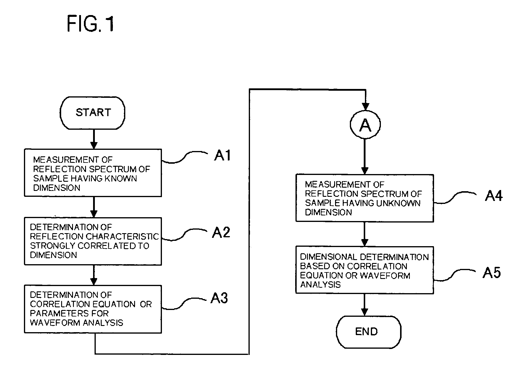
[0106]FIG. 6 shows a block diagram showing a configuration of one embodiment of the periodic structure measurement apparatus of the present invention. FIG. 7 is a flow chart explaining calculation procedures in Example of the method of measuring a micro-structure of the present invention. Referring now to FIG. 6, this Example is configured as having a sample stage 2 on which the measurement sample 1 is placed, a measuring beam source 4, such as a halogen lamp, supplying the measuring beam, a photo-detector 6 allowing the measuring beam to normally irradiate the sample and spectrally measuring the reflected light from the sample, and a calculator 7 processing data obtained by the photo-detector 6.

[0107] The periodic structure is measured by measuring wavelength de...

example 2

[0152] The next paragraphs will detail a second example of the present invention.

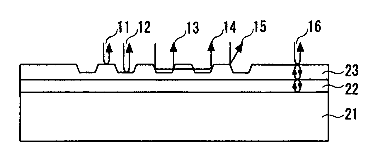
[0153]FIG. 11 is a sectional view showing a geometry of a micro-structure and reflection characteristics under irradiation with the measuring beam in Example 2 of the method of measuring a micro-structure according to the present invention. The configuration shown in FIG. 11 differs from that of Example 1, in that semiconductor layers A 22 and B 23 are formed on a semiconductor substrate 21, and the periodic micro-structure is formed on the semiconductor layer B 23.

[0154] As the reflected light obtained upon irradiation with the measuring beam, it is necessary in this Example to take: [0155] reflection at the interface between the substrate and the semiconductor layer A; and [0156] reflection at the interface between the semiconductor layer A and semiconductor layer B;

into consideration together with the reflection on the surface of the substrate, as indicated by a reflected light 16 on the flat por...

example 3

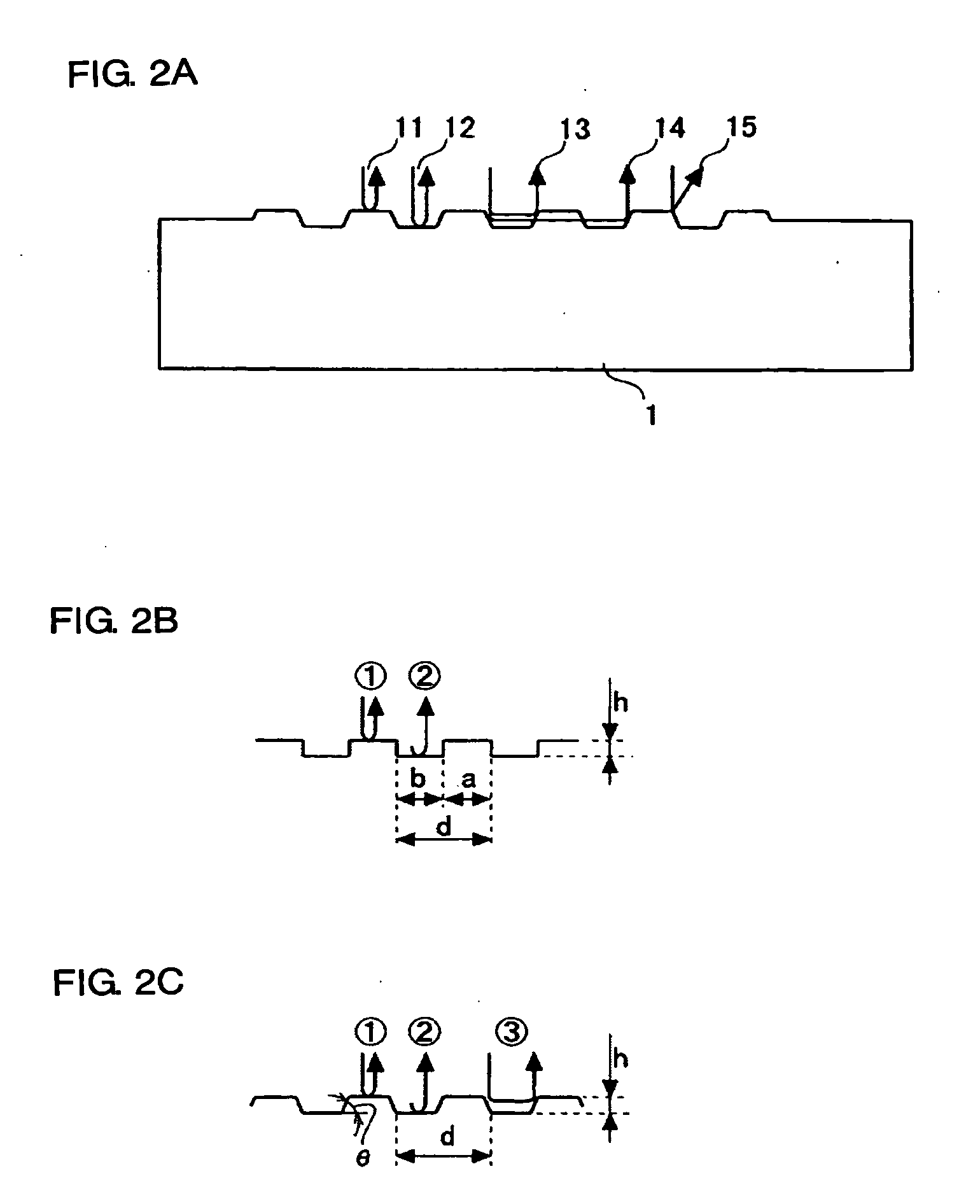
[0178] Next paragraphs will detail Example 3 of the present invention, referring to the attached drawings.

[0179] As described in Example 1, the reflection spectrum obtained upon irradiation with the measuring beam onto the micro-structure is strongly affected by the geometry, and is reflected into the peak wavelength, intensity and so forth. Mathematical expression of the features (wavelength parameters) of the reflection spectrum therefore makes it possible to indicate dimension to be controlled.

[0180]FIG. 13 is a sectional view showing a geometry of a micro-structure and reflection characteristics of a measuring beam observed in a sample measurement according to Example 3 of the method of measuring a micro-structure of the present invention. The configuration shown in FIG. 13 differs from that of Example 2, in that the semiconductor layers A 22 and B 23 are formed on the semiconductor substrate 21, the periodic micro-structure is formed on the semiconductor layer B 23, and a sem...


PUM


Abstract

This invention provides a method and an apparatus of measuring a micro-structure, capable of evaluating a geometry of a micro-structure formed typically on the surface of a semiconductor substrate, in a non-destructive, easy, precise and quantitative manner. A reflection spectrum of a sample having a known dimension of a target micro-geometry is measured (A1), features (waveform parameters) which strongly correlate to a dimension of the measured micro-geometry are determined (A2), a relation between the dimension of the micro-geometry and the waveform parameters is found (A3), and a dimension of the micro-structure having an unknown dimension is finally determined using this relation and based on the reflection spectrum obtained therefrom (A4, A5).

Description

[0001] This application is based on Japanese patent application No. 2004-105903 the content of which is incorporated hereinto by reference. DISCLOSURE OF THE INVENTION [0002] 1. Field of the Invention [0003] The present invention relates to a method of measuring a micro-structure, a micro-structure measurement apparatus, and a micro-structure analytical system, and in particular to a method of measuring a micro-structure, a micro-structure measurement apparatus, and a micro-structure analytical system preferably applicable to optical measurement of structures of nanometer level. [0004] 2. Related Art [0005] It has conventionally been important in semiconductor fabrication processes such as lithography, etching and so forth, aimed at forming fine patterns of a 0.1 μm (micrometer) level, to precisely control dimensions of the patterns at the nanometer level, so that it has been believed as essential to readily and precisely measure dimensions of the patterns, when conditions for the l...

Claims


Application Information

Patent Timeline
IPC IPC(8): G01B11/02G01B9/02G01B11/24H01L21/66
CPCG01B11/24
Inventor MUROYA, YOSHIHARU
Owner NEC ELECTRONICS CORP
Why Eureka
Try Eureka