Microelectronic assembly with underchip optical window, and method for forming same

Inactive Publication Date: 2005-10-13
DELPHI TECH INC
View PDF6 Cites 12 Cited by
  • Summary
  • Abstract
  • Description
  • Claims
  • Application Information

AI Technical Summary

Benefits of technology

[0006] In accordance with this invention, a microelectronic assembly comprises an integrated circuit die mounted on a substrate by a plurality of bump interconnections. The die includes an active face having a central region surrounded by a perimeter region, and is arranged relative to the substrate such that the active face faces the substrate and is spaced apart by a gap. The bump interconnections are bonded to the perimeter region of the die and to the substrate, to thereby attach the die to the substrate. The assembly also includes a polymeric encapsulant about the die on the substrate and extending into the gap to encapsulate the interconnections. The encapsulant defines an optical window within the gap underlying the central region. It is an advantage of this invention that the window allows optical access to the active face of the die, including the optical sensors thereon. Moreover, the assembly may be formed using an encapsulant having a desired CTE that is adjusted for protecting the bump interconnections from thermally induced stress.
[0007] In one aspect of this invention a method is provided for forming a microelectronic assembly having an overmolded polymeric encapsulant that define

Problems solved by technology

This thermally induced stress, if not for the encapsulant, would cause fatigue in the solder and lead to fracture of the interconnections and

Method used


Image

  • Microelectronic assembly with underchip optical window, and method for forming same
  • Microelectronic assembly with underchip optical window, and method for forming same
  • Microelectronic assembly with underchip optical window, and method for forming same

Examples


Embodiment Construction

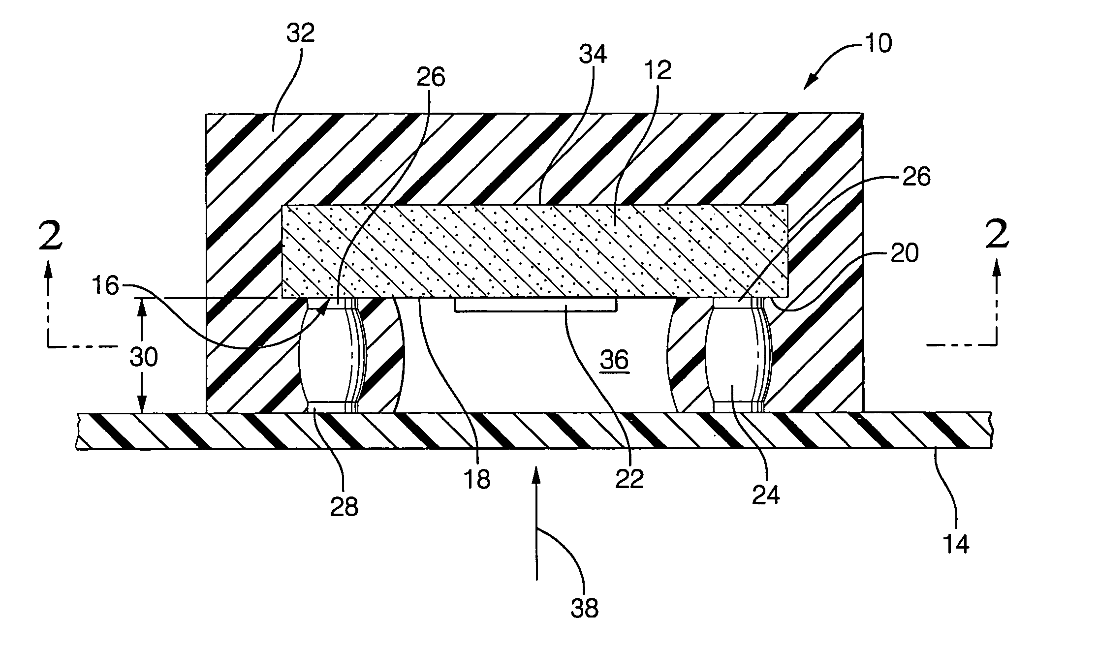
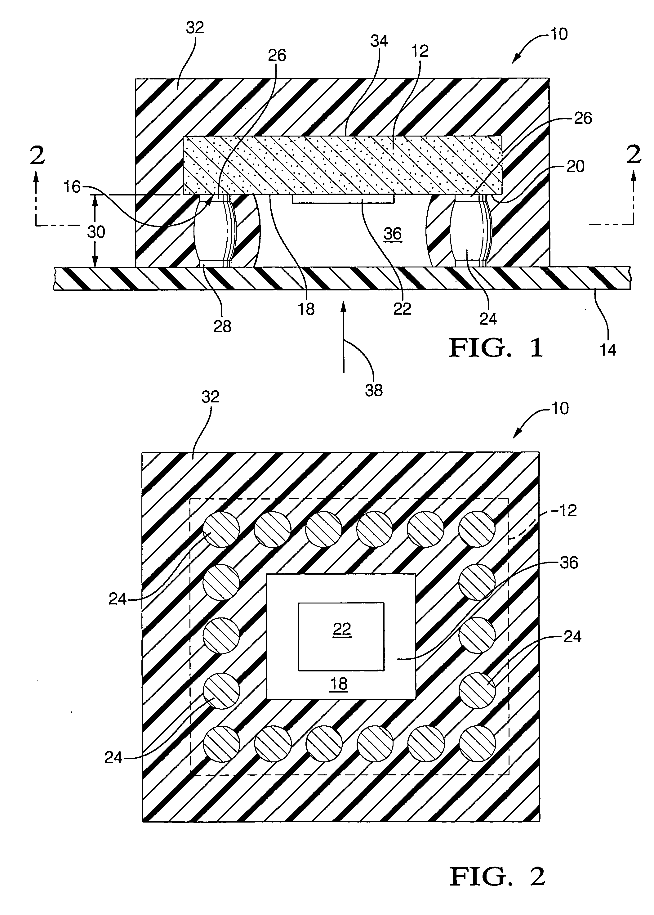
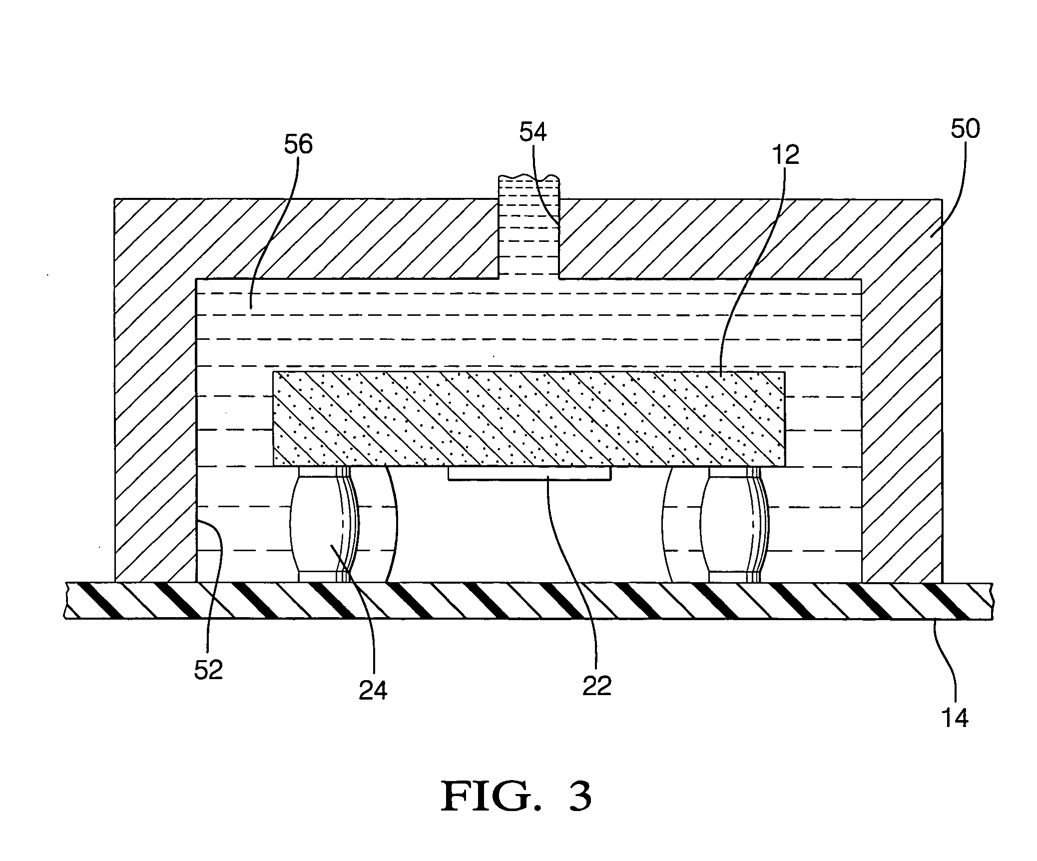
[0013] In accordance with a preferred embodiment of this invention, referring to FIGS. 1 and 2, a microelectronic assembly 10 comprises an integrated circuit die 12 mounted onto a substrate 14 in a flip chip arrangement. Substrate 14 is formed of a transparent material. A preferred material is glass. Alternately, the substrate may be formed of a polymeric thin film or a polymer glass laminate, such as an FR4 board. Die 12 is formed of a semiconductor material, preferably silicon, and comprises an active face 16 that includes a central region 18 surrounded by a perimeter region 20. An optical feature 22 is formed on the active face at the central region. In a preferred embodiment, die 12 may be an digital imaging device that includes, as feature 22, an array of optical sensors and related circuitry for sensing and processing light to produce an image, such as a digital picture. Alternately, feature 22 may be detector for receiving an optical signal, or an element for emitting an opti...


PUM


Abstract

A microelectronic assembly includes an integrated circuit die spaced apart from a substrate and connected by bump interconnections, and an polymeric encapsulant molded about the die. The encapsulant extends into the gap about the interconnections, but is confined to the perimeter so as to define an underchip optical window adjacent the central region of the die. The window allows optical access to the active face of the die, including to optical sensors thereon. During manufacture of the assembly, following attachment of the die on the substrate, a molding cavity is positioned about the die on the substrate. Polymeric material is injected into the cavity at a pressure effective to initiate flow into the gap about the solder bump interconnections. The pressure is then reduced to prevent flow of the polymeric material into the central region.

Description

TECHNICAL FIELD OF INVENTION [0001] This invention relates to a microelectronic assembly that includes an integrated circuit die attached to a substrate by solder bump interconnections. More particularly, this invention relates to such assembly that includes an overmolded polymeric encapsulant that extends within a gap between the integrated circuit die and the substrate to protect the solder bump interconnections and further that defines an optical window to allow the integrated circuit device to receive and emit optical signals through the substrate. BACKGROUND OF INVENTION [0002] A typical flip chip microelectronic assembly comprises an integrated circuit die, also commonly referred to as a chip, mounted on a substrate, such as a printed circuit board, by solder bump interconnections that physically attach the chip to the substrate and also form electrical connections for conducting electrical signals to and from the chip for processing. To form the assembly, solder bumps are aff...

Claims


Application Information

Patent Timeline
IPC IPC(8): H01L23/29H01L23/31H01L27/146H01L33/54
CPCH01L23/293H01L23/315H01L23/3185H01L27/14618H01L31/0203H01L33/54H01L2224/16225H01L2224/05573H01L2224/05568H01L2924/00014H01L2224/05599H01L2224/06135
Inventor BRANDENBURG, SCOTT D.TSAI, JEENHUEI S.BURNS, JEFFREY H.
Owner DELPHI TECH INC
Why Eureka
Try Eureka