Clock selection circuit and digital processing system for reducing glitches

Inactive Publication Date: 2005-10-13
SAMSUNG ELECTRONICS CO LTD
View PDF5 Cites 43 Cited by
  • Summary
  • Abstract
  • Description
  • Claims
  • Application Information

AI Technical Summary

Benefits of technology

[0008] Exemplary embodiments of the present invention may provide a clock selection circuit that reduces the likelihood of glitches when performing a clock selection operation and/or

Problems solved by technology

Conventional clock selection circuits that perform clock selection operations may have a high lev

Method used


Image

  • Clock selection circuit and digital processing system for reducing glitches
  • Clock selection circuit and digital processing system for reducing glitches
  • Clock selection circuit and digital processing system for reducing glitches

Examples


Embodiment Construction

[0031] Hereinafter, the present invention will be described in detail by explaining exemplary embodiments of the invention with reference to the attached drawings. Like reference numerals in the drawings may represent like elements.

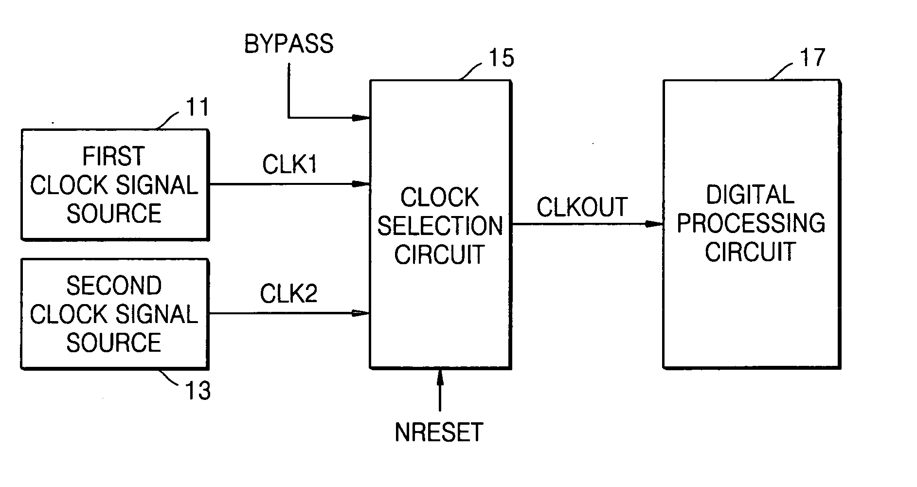
[0032]FIG. 1 is a block diagram of a digital processing system according to an exemplary embodiment of the present invention. Referring to FIG. 1, the digital processing system may include a first clock signal source 11, a second clock signal source 13, a clock selection circuit 15 and a digital processing circuit 17.

[0033] The first clock signal source 11 may generate a first clock signal CLK1, and the second clock signal source 13 may generate a second clock signal CLK2. The first and second clock signal sources may be internal or external clock signal sources.

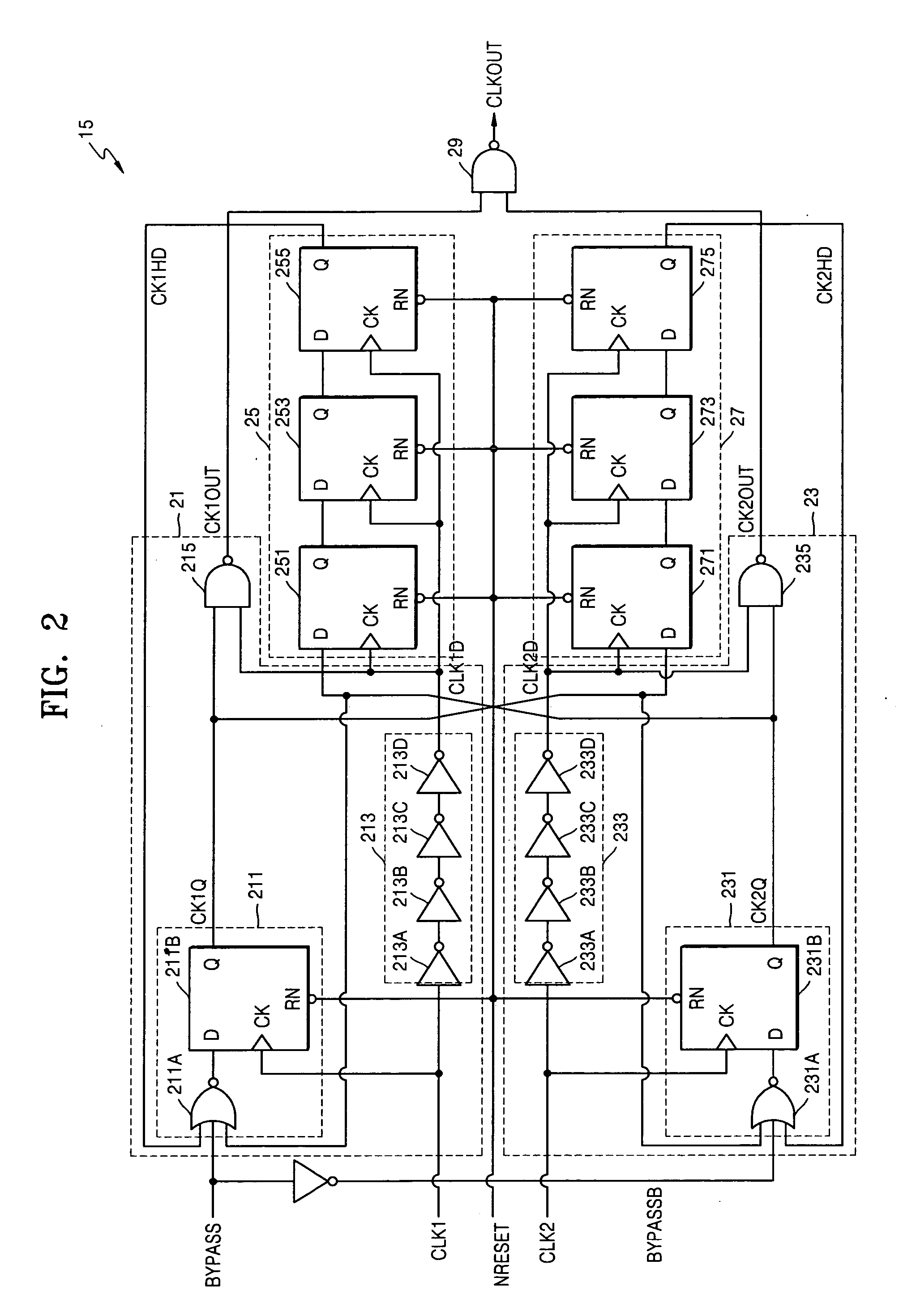
[0034] The clock selection circuit 15, according to an exemplary embodiment of the present invention, may select one of the first and second clock signals CLK1 and CLK2 as an output clock signa...


PUM


Abstract

A clock selection circuit and method may operate to generate a clock signal for a digital processing system. In the clock selection circuit, first and second clock control signals may be generated based on a received control signal and/or the inverse of a received clock signal. A first clock signal may be selected when the first clock control signal is activated, and may be output as the selected clock signal. A second clock signal may be selected when the second clock control signal is activated, and may be output as the selected clock signal. The selection operation of the clock selection circuit may reduce the likelihood that a glitch occurs and/or may reduce the amount of power consumed when compared to a conventional clock selection circuit.

Description

BACKGROUND OF THE INVENTION [0001] This application claims the priority of Korean Patent Application No. 2004-24889, filed on Apr. 12, 2004, in the Korean Intellectual Property Office, the disclosure of which is incorporated by reference herein in its entirety. [0002] 1. Field of the Invention [0003] The present invention relates to a digital processing system which may include two or more clock signal sources, and more particularly, to a clock selection circuit that selects one clock signal from two or more clock signals and outputs the selected clock signal. [0004] 2. Description of the Related Art [0005] For certain types of semiconductor circuits, speed and capacity has increased. Some examples of these types of semiconductor circuits may include, for example, application specific integrated circuits (ASIC), central processing units (CPU), and digital signal processors (DSP). Some of the progress in the speed and capacity of semiconductor circuits may be attributed to system-on-...

Claims


Application Information

Patent Timeline
IPC IPC(8): G06F1/04H03K3/00G06F1/10G06F1/32
CPCG06F1/10G06F1/32G06F1/04
Inventor RHEE, YOUNG-CHUL
Owner SAMSUNG ELECTRONICS CO LTD
Why Eureka
Try Eureka