Solid-state color image pickup apparatus with a wide dynamic range, and digital camera on which the solid-state image pickup apparatus is mounted

a pickup apparatus and color image technology, applied in the direction of television system scanning details, radioation control devices, television systems, etc., can solve the problems of reducing resolution, false color, and inability to increase the area of light receiving portions, so as to achieve the effect of widening the dynamic rang

Inactive Publication Date: 2005-10-13
FUJIFILM CORP
View PDF19 Cites 81 Cited by
  • Summary
  • Abstract
  • Description
  • Claims
  • Application Information

AI Technical Summary

Benefits of technology

[0013] It is an object of the invention to provide a solid-state color image pickup apparatus which is configured so that each pixel detects photoelectric conversion signals of plural colors, and in which the dynamic range can be widened, and also to provide a digital camera on which such a solid-state image pickup apparatus is mounted.

Problems solved by technology

In the related-art solid-state image pickup apparatus, therefore, many light receiving portions and signal read circuits must be formed on the same surface of a semiconductor substrate, thereby producing a problem in that the area for the light receiving portions cannot be increased.
This causes a false color, and reduces the resolution.
Furthermore, blue light and green light incident on a light receiving portion where a red color filter is formed does not contribute to photoelectric conversion, but is absorbed as heat into the color filter, thereby producing another problem in that the light use efficiency is poor and the sensitivity is low.
As described above, the related-art solid-state image pickup apparatus has various problems.
Consequently, a CCD device and a CMOS device are hardly expected to configure an image sensor which can solve the above-discussed problems, and which is superior in image quality and sensitivity than the related-art one.
When the number of pixels is increased, however, the amount of signal charges which can be detected by each pixel is reduced, thereby causing a further problem in that the dynamic range is lowered.

Method used


Image

  • Solid-state color image pickup apparatus with a wide dynamic range, and digital camera on which the solid-state image pickup apparatus is mounted
  • Solid-state color image pickup apparatus with a wide dynamic range, and digital camera on which the solid-state image pickup apparatus is mounted
  • Solid-state color image pickup apparatus with a wide dynamic range, and digital camera on which the solid-state image pickup apparatus is mounted

Examples


first embodiment

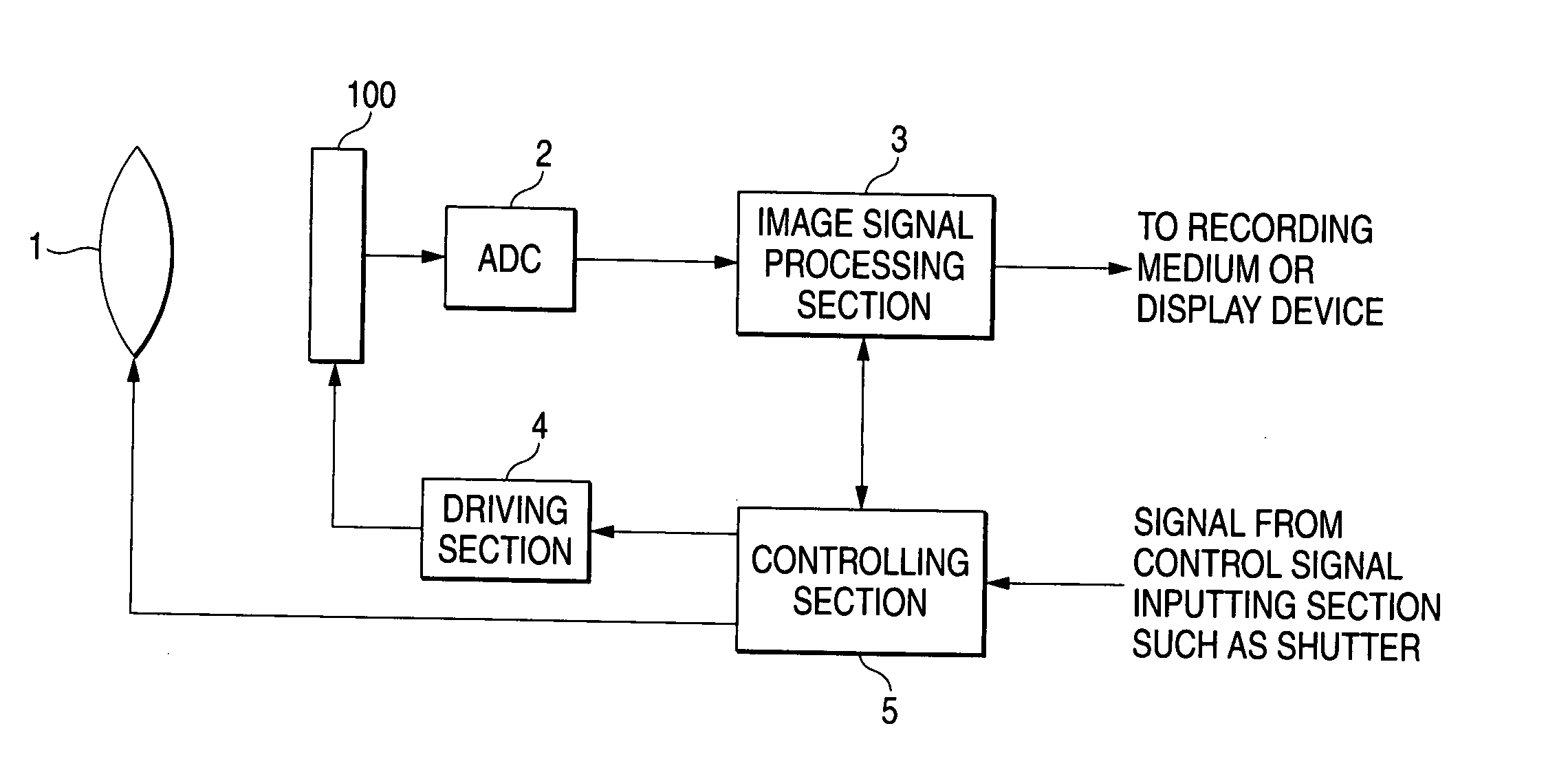
[0044]FIG. 1 is a block diagram of a digital camera on which a solid-state color image pickup apparatus of the photoelectric converting film stack type of a first embodiment of the invention is mounted. The digital camera comprises: an imaging optical system 1 including an imaging lens, an aperture, and a shutter; the solid-state color image pickup apparatus 100 of the photoelectric converting film stack type which will be described later in detail; an analog / digital converter 2 which converts an analog image signal output from the photoelectric converting film stack type solid-state color image pickup apparatus 100, to a digital signal; an image signal processing section 3 which applies image processing on the digital image signal, and which stores the processed signal onto a recording medium, or displays it on a display device; a driving section 4 which controls the operation of the photoelectric converting film stack type solid-state color image pickup apparatus 100; and a contro...

second embodiment

[0098]FIG. 7 is a surface diagram of a photoelectric converting film stack type solid-state color image pickup apparatus of a second embodiment of the invention, and corresponds to FIG. 4 of the first embodiment. FIG. 8 is a surface diagram of vertical transfer paths formed on the surface of the semiconductor substrate, and showing a portion corresponding to four pixels (two higher-sensitivity pixels×two lower-sensitivity pixels). FIG. 8 corresponds to FIG. 6 of the first embodiment.

[0099] The second embodiment is characterized in that the positions to which the longitudinal lines 31b, 31g, 31r disposed in each of the higher-sensitivity pixels 101 are downward elongated, i.e., the vertical positions of the signal charge accumulating regions 33b, 33g, 33r are shifted by a distance corresponding to two transfer electrode regions from the vertical positions where the signal charge accumulating regions 34b, 34g, 34r to which the longitudinal lines 32b, 32g, 32r disposed in each of the ...

third embodiment

[0107]FIG. 10 is a circuit diagram of signal read circuits of a photoelectric converting film stack type solid-state color image pickup apparatus of a third embodiment of the invention. In the photoelectric converting film stack type solid-state color image pickup apparatuss of the first and second embodiments, the signal read circuits disposed in the semiconductor substrate are configured by charge-coupled elements (the vertical transfer paths and the horizontal transfer path). In the present embodiment, the signal read circuits are configured by MOS transistor circuits.

[0108]FIG. 10 shows signal read circuits for two higher-sensitivity pixels×two lower-sensitivity pixels. For each pixel, circuits for respectively reading out blue, green, and red signals are disposed, and hence twelve signal read circuits are disposed in total. The signal read circuits have the same configuration. Therefore, the following description will be made only on one of the signal read circuits, and descri...


PUM


Abstract

A solid-state color image pickup apparatus comprises a plurality of pixels, wherein said plurality of pixels are arranged to form an array pattern comprising a first checkered pattern and a second checkered pattern, wherein each of said plurality of pixels detects colors signals of red, green, and blue, and wherein said plurality of pixels comprises: higher-sensitivity pixels forming the first checkered pattern; and lower-sensitivity pixels forming the second checkered pattern.

Description

BACKGROUND OF THE INVENTION [0001] 1. Field of the Invention [0002] The present invention relates to a solid-state color image pickup apparatus with a wide dynamic range, and a digital camera on which the solid-state image pickup apparatus is mounted. [0003] 2. Description of the Related Art [0004] In a CCD solid-state image pickup apparatus or a CMOS solid-state image pickup apparatus which is mounted on a digital camera, a large number of photoelectric converting elements (photodiodes) serving as light receiving portions, and signal read circuits which read out photoelectric conversion signals obtained in the photoelectric converting elements are formed on the surface of a semiconductor substrate. The signal read circuits are configured by, in the case of a CCD device, charge transfer circuits and transfer electrodes, and, in the case of a CMOS device, MOS circuits and signal lines. [0005] In the related-art solid-state image pickup apparatus, therefore, many light receiving porti...

Claims


Application Information

Patent Timeline
Patent Type & Authority Applications(United States)
IPC IPC(8): H01L27/14H01L27/146H01L31/10H04N9/07H04N101/00
CPCH04N3/155H04N25/585
Inventor SUZUKI, NOBUO
Owner FUJIFILM CORP
Why Eureka
Try Eureka