Display device

a technology of a display device and a display terminal, which is applied in the direction of semiconductor devices, instruments, constructions, etc., can solve the problems of not being able to directly connect the output terminals of the semiconductor device and the electrodes of the glass substrate, and not being able to directly attach all the semiconductor devices, so as to achieve the effect of dissipating hea

Inactive Publication Date: 2005-10-20
FUJITSU HITACHI PLASMA DISPLAY LTD
View PDF12 Cites 22 Cited by
  • Summary
  • Abstract
  • Description
  • Claims
  • Application Information

AI Technical Summary

Benefits of technology

[0009] An object of the present invention is to provide a drive circuit module and a display device capable of dissipating

Problems solved by technology

As a semiconductor device produces a large amount of heat, there may be a need to dissipate heat produced by a semiconductor device.
When the glass substrate has a small number of electrodes, it may be possible to directly connect the output terminals of the semiconductor device and the electrodes of the glass substrate, but when the glass substrate has a large number of electrodes, it is not possibl

Method used


Image

  • Display device
  • Display device
  • Display device

Examples


first embodiment

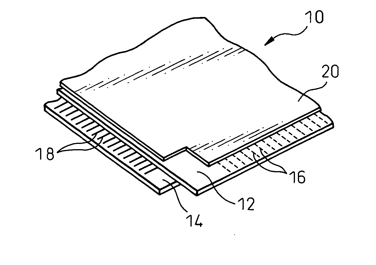
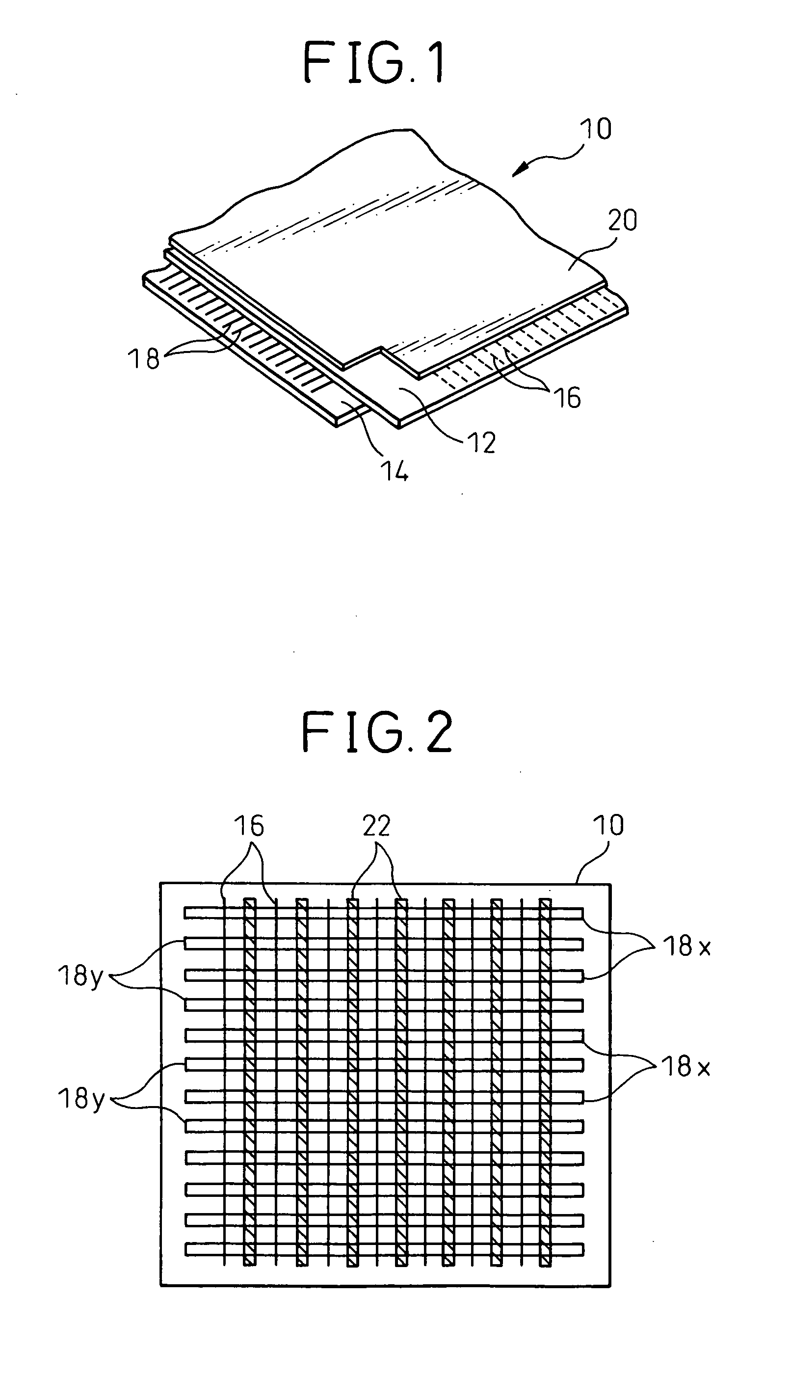
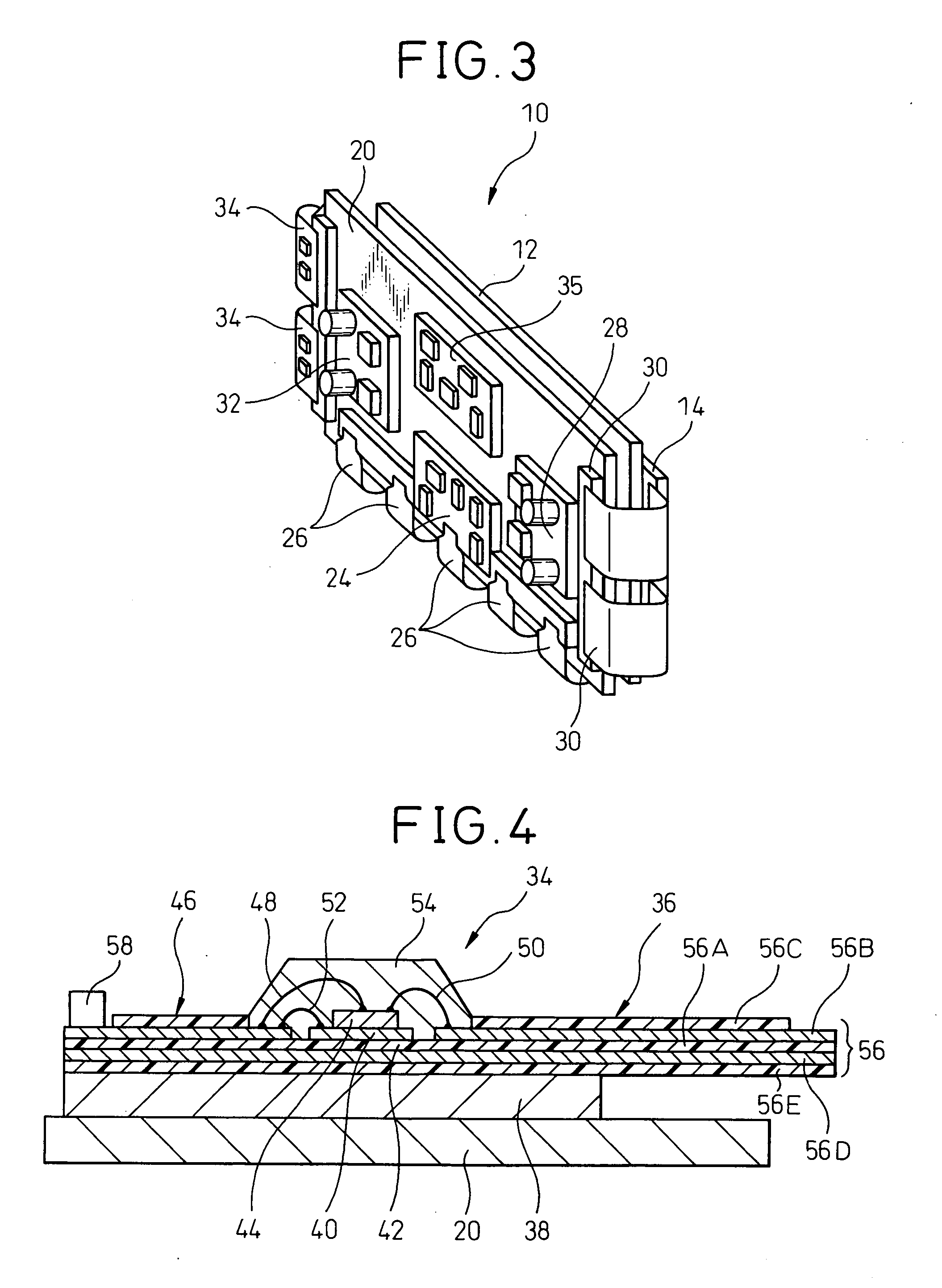
[0051] Embodiments of the present invention are described below with reference to the drawings. FIG. 1 is a substantially perspective view showing a part of a plasma display device according to the present invention. FIG. 2 is a diagram showing an arrangement of electrodes in the plasma display device in FIG. 1. FIG. 3 is a substantially perspective view showing the plasma display device in FIG. 1 including a circuit board. Although the present invention is described below while taking a plasma display device as an example, the present invention is not limited to a plasma display device but can be applied to other display devices having a plurality of drive electrodes such as an LCD, an EL Display, or an FED.

[0052] A plasma display device 10 comprises a pair of glass substrates 12 and 14 in opposition to each other, a chassis 20 fixed on the glass substrate 12, which is one of the glass substrates, and a drive circuit arranged on the chassis 20. The glass substrate 12 has a pluralit...

second embodiment

[0089]FIG. 16 is a sectional view showing a variation example of the scan drive circuit module 34 shown in FIG. 15. The scan drive circuit module 34 comprises the flexible circuit board 36 connected to the Y electrodes 18y, the wiring pattern 46, the heat dissipation plate 38, the insulation layer 42, and the semiconductor device (semiconductor chip) 44 mounted on the heat dissipation plate 38 via the insulation layer 42. The heat dissipation plate 38 is made of a metal plate having a high heat conductivity such as an aluminum plate. The input terminals of the semiconductor device 44 are electrically connected to the wiring pattern 46 and the output terminals of the semiconductor device 44 are electrically connected to the wiring pattern of the flexible circuit board 36.

[0090] The wiring pattern 46 is formed as a conductive layer of the rigid circuit board 74. The rigid circuit board 74 comprises the base film 74A, the conductive layer 74B formed at one side of the base film 74A, a...

third embodiment

[0096]FIG. 18 is a sectional view showing the scan drive circuit module 34 according to the present invention. FIG. 19 is a diagram showing the insertion of the connector shown in FIG. 18 into the counterpart connector. The scan drive circuit module 34 comprises the flexible circuit board 36 connected to the Y electrodes 18y, the wiring pattern 46, the heat dissipation plate 38, the insulation layer 42, and the semiconductor device (semiconductor chip) 44 mounted on the heat dissipation plate 38 via the insulation layer 42. The heat dissipation plate 38 is made of a metal plate having a high heat conductivity such as an aluminum plate. The input terminals of the semiconductor device 44 are electrically connected to the wiring pattern 46 and the output terminals of the semiconductor device 44 are electrically connected to the wiring pattern of the flexible circuit board 36.

[0097] The wiring pattern 46 is formed as a conductive layer of the rigid circuit board 74. The configuration of...


PUM


Abstract

A drive circuit module capable of dissipating heat produced by a semiconductor device, in the form of a bare chip, and in which the semiconductor device can be driven in a floating state, and a display device in which the drive circuit module is mounted have been disclosed. The drive circuit module comprises a heat dissipation plate, a flexible circuit board, an insulation layer having a wiring pattern, a semiconductor device mounting insulation layer, and a semiconductor device mounted on the heat dissipation plate via the semiconductor device mounting insulation layer, in which the insulation layer having the wiring pattern and the semiconductor device mounting insulation layer are made of a non-conductive resin, the flexible circuit board and the insulation layer having the wiring pattern are fixed on the heat dissipation plate directly or indirectly, and the semiconductor device is electrically connected to the wiring pattern and the flexible circuit board.

Description

BACKGROUND OF THE INVENTION [0001] 1. Technical Field [0002] The present invention relates to a display device, such as a plasma display device, and to a drive circuit module. [0003] 2. Related Art [0004] As described in EP 1006505, U.S. Pat. No. 6,703,792, U.S. Pat. No. 6,407,508, and U.S. Pat. No. 6,703,702, a plasma display device comprises a pair of glass substrates each having a plurality of electrodes. A plasma display device has three kinds of electrodes. For example, the three kinds of electrode include a plurality of address electrodes parallel to each other and a plurality of X electrodes and a plurality of Y electrodes arranged by turns in parallel to the direction perpendicular to the address electrodes. [0005] The address electrode is connected to an address pulse generation circuit via an address drive circuit module, the X electrode is connected to an X electrode sustain pulse generation circuit via a sustain drive circuit module, and the Y electrode is connected to a...

Claims


Application Information

Patent Timeline
IPC IPC(8): G09G3/294H01L23/31H01L23/36H01L23/367H01L23/373H01L23/40H01L23/538
CPCG09G3/294H01L2924/014G09G2330/045G09G2330/06H01L23/3121H01L23/36H01L23/3735H01L23/5386H01L24/49H01L2224/48091H01L2224/49109H01L2224/49171H01L2924/01013H01L2924/01029H01L2924/01033H01L2924/01047H01L2924/0105H01L2924/01079H01L2924/13091H01L2924/14H01L2924/15153H01L2924/1517H01L2924/19041H01L2924/19107G09G2300/0408H01L24/48H01L2924/00014H01L2924/181H01L2224/45099H01L2924/00012E02D29/12
Inventor OHNO, TAIZOUOKADA, YOSHINORIUMEHARA, KUNIOKANAZAWA, YOSHIKAZUKISHI, TOMOKATSUKOIZUMI, HARUOKOBAYASHI, TAKAYUKISANO, YUJI
Owner FUJITSU HITACHI PLASMA DISPLAY LTD
Why Eureka
Try Eureka