
Routing architecture with high speed I/O bypass path

a routing architecture and bypass path technology, applied in the field of routing architectures, can solve the problems of large propagation delay and achieve the effects of reducing delays, facilitating connections, and facilitating routing of output signals through one or more channels

Inactive Publication Date: 2005-10-20
ALTERA CORP
View PDF7 Cites 7 Cited by
  • Summary
  • Abstract
  • Description
  • Claims
  • Application Information

AI Technical Summary

Benefits of technology

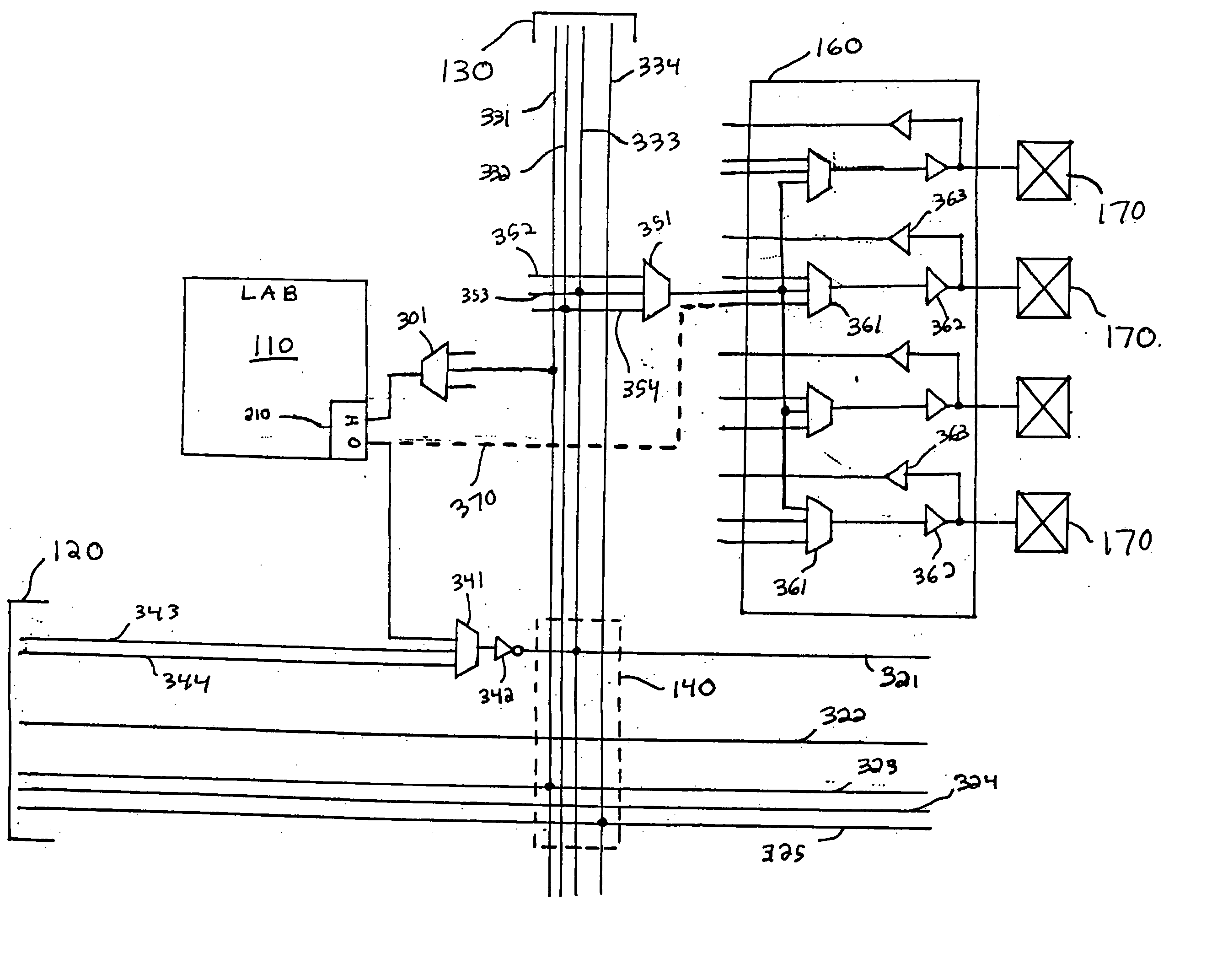
[0009] An output bypass path according to the principles of the present invention adds a direct connection between an LE output and I / O block circuitry in a PLD for reducing the delays associated with providing signals from the LE to circuitry external to the PLD. In one embodiment, the output bypass path is used for directly connecting the LE output to the input of an I / O multiplexer of the I / O block. In this manner, the delays associated with routing an LE output signal through one or more multiplexers, drivers and / or conductors are eliminated or at least significantly reduced. In another embodiment, the output bypass path provides a direct connection between the LE output and I / O block circuitry that also bypasses the I / O multiplexer. In particular, this output bypass path provides a direct connection between the LE output and an I / O block bypass multiplexer (which in this embodiment is necessary to select as its output the signal from either the I / O multiplexer or the output bypass path).
[0010] Also provided in accordance with the principles of the present invention is an input bypass path which provides direct connections between an input buffer of an I / O block and an otherwise dangling segmented conductor at the periphery, or boundary, of the PLD's routing architecture. Accordingly, the input bypass path eliminates or at least reduces the delays associated with using an input multiplexer and driver for routing a signal from the I / O block onto a signal conductor of the PLD routing architecture.

Problems solved by technology

Meanwhile, each of these components adds a respective delay to the signal transfer process, sometimes resulting in a prohibitively large propagation delay (e.g., the pin-to-pin data transfer speed may not be fast enough to support certain applications) for the PLD.

Method used


Image

  • Routing architecture with high speed I/O bypass path
  • Routing architecture with high speed I/O bypass path
  • Routing architecture with high speed I/O bypass path

Examples


Embodiment Construction

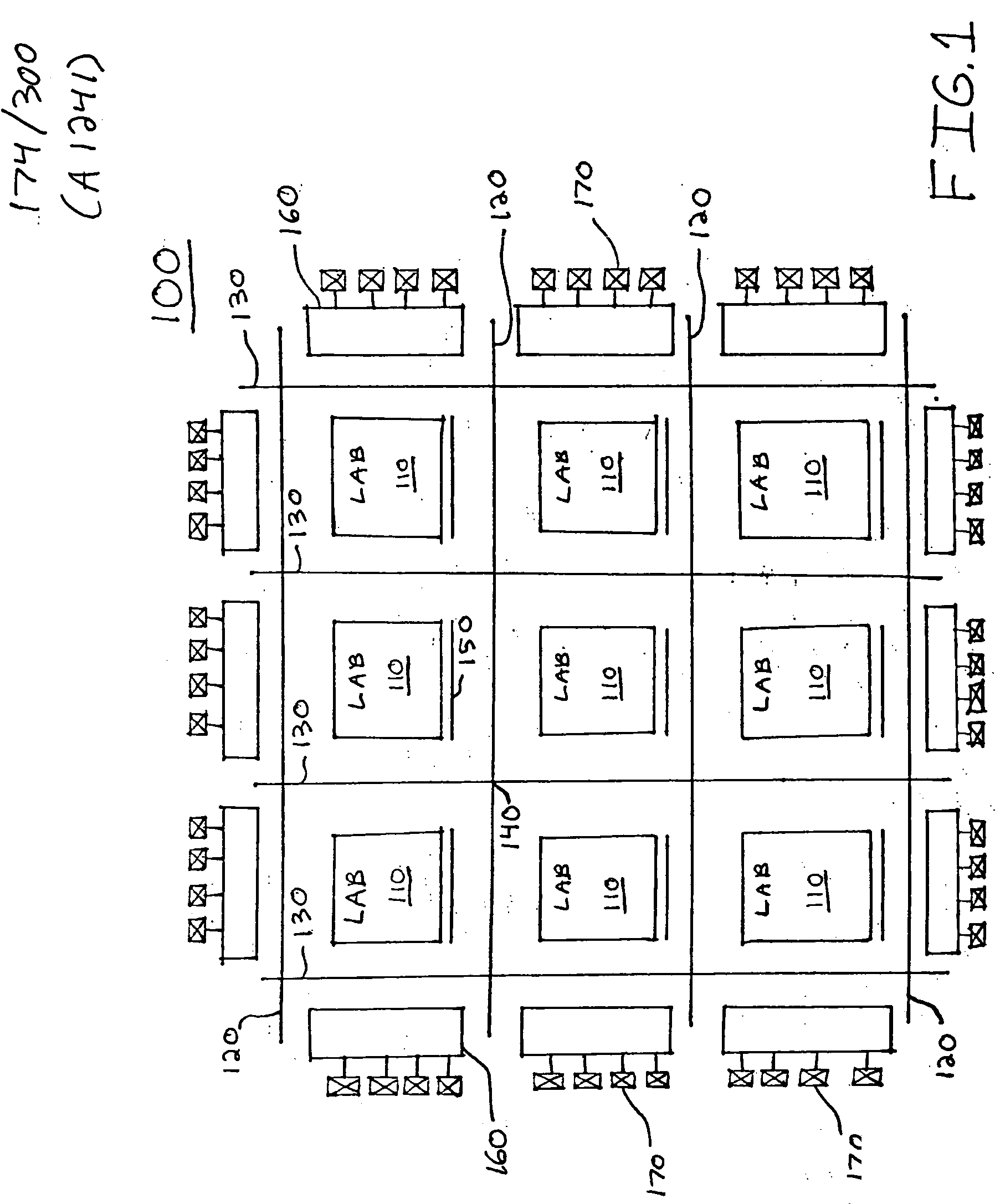
[0023]FIG. 1 is a simplified block diagram showing the overall routing architecture of a PLD 100 which incorporates the principles of present invention. Many details of PLD architecture, organization, and circuit design are well known and therefore not necessary to be shown or described for an understanding of the present invention. Such details have generally been omitted from FIG. 1 and the remaining figures described below for the purpose of simplifying the description of the present invention.

[0024] As illustrated in FIG. 1, PLD 100 includes a three-by-three two-dimensional array of nine LABs 110. However, PLD 100 may contain any arbitrary number of LABs 110 (e.g., more or less nine). Moreover, it will also be understood that LABs 110 need not be organized in a square matrix, or array, as illustrated in FIG. 1. Rather, for example, PLD 100 may include a one-by-nine matrix of LABs 110. The invention is not limited in either of these manners.

[0025] The routing architecture of PL...


PUM


Abstract

Improved routing architectures including one or more high speed input / output (I / O) bypass paths are provided for use in, for example, programmable logic devices (PLDs) such as field programmable gate arrays (FPGAs). The output bypass paths add additional routing connections to the routing architecture, providing faster connections between the output of a logic element (LE) in the PLD and external circuitry. In one embodiment, an output bypass path is used for directly connecting the output of the LE to the input of an I / O multiplexer of an I / O block. In another embodiment, the output bypass path also bypasses the I / O multiplexer, providing a direct connection between the output of the LE and a bypass multiplexer of the I / O block. Also provided is an input bypass path which provides direct connections between an input buffer of the I / O block and an otherwise dangling conductor at the periphery of the PLD's routing architecture.

Description

BACKGROUND OF THE INVENTION [0001] The present invention relates generally to routing architectures for use in, for example, programmable logic devices (PLDs). More particularly, this invention relates to improved routing architectures using one or more high speed input / output (I / O) bypass paths. [0002] PLDs are well known as is shown, for example, by Jefferson et al. U.S. Pat. No. 6,215,326 and Ngai et al. U.S. Pat. No. 6,407,576. In general, a PLD is a general-purpose integrated circuit device that is programmable to perform any of a wide range of logic tasks. Instead of having to design and build separate logic circuits for performing different logic tasks, general-purpose PLDs can be programmed in various different ways to perform those different logic tasks. Many manufacturers of electronic circuitry and systems find the use of PLDs to be an advantageous way to provide various components of what they need to produce. For the purposes of this description, the term PLD encompasse...

Claims


Application Information

Patent Timeline
Patent Type & Authority Applications(United States)
IPC IPC(8): H03K19/177
CPCH03K19/17736H03K19/17792H03K19/17744
Inventor VEST, WILLIAM BRADLEYLEVENTIS, PAUL
Owner ALTERA CORP
Learn More