Antenna switch circuit, and composite high frequency part and mobile communication device using the same

a switch circuit and high frequency technology, applied in the direction of carpet cleaning, floor surfacing/polishing machines, pulse techniques, etc., can solve the problem that the mobile phone is not suitable for a mobile application, and achieve the effect of small size, light weight and high isolation characteristi

Inactive Publication Date: 2005-10-20
PANASONIC CORP
View PDF4 Cites 29 Cited by
  • Summary
  • Abstract
  • Description
  • Claims
  • Application Information

AI Technical Summary

Benefits of technology

[0036] According to the second to the fourth aspects of the present invention, the antenna switch circuit is also used, so that the effect similar to that of the above antenna switch circuit may be provided.
[0037] As described above, according to the present invention, the small-sized and lightweight antenna switch circuit can be provided even when the mobile phone is applied in a multiband application, so that it is possible to contribute to realizing a mobile phone which is small in size and light in weight and is compatible with the multiband application. Further, by proving the series resonant circuit in the shunt circuit, it is possible to realize the isolation characteristic that is higher than that of the related art. Furthermore, since a plurality of series resonant circuits (e.g., two series resonant circuits) are provided in parallel, the higher isolation characteristic across the wider band is realized, thus contributing to reduce the size and improve a performance of the device.

Problems solved by technology

However, both of the volume and the weight of the mobile phone are increased in proportion to the number of communication systems, so that such a mobile phone is not suitable for a mobile application.

Method used


Image

  • Antenna switch circuit, and composite high frequency part and mobile communication device using the same
  • Antenna switch circuit, and composite high frequency part and mobile communication device using the same
  • Antenna switch circuit, and composite high frequency part and mobile communication device using the same

Examples


first embodiment

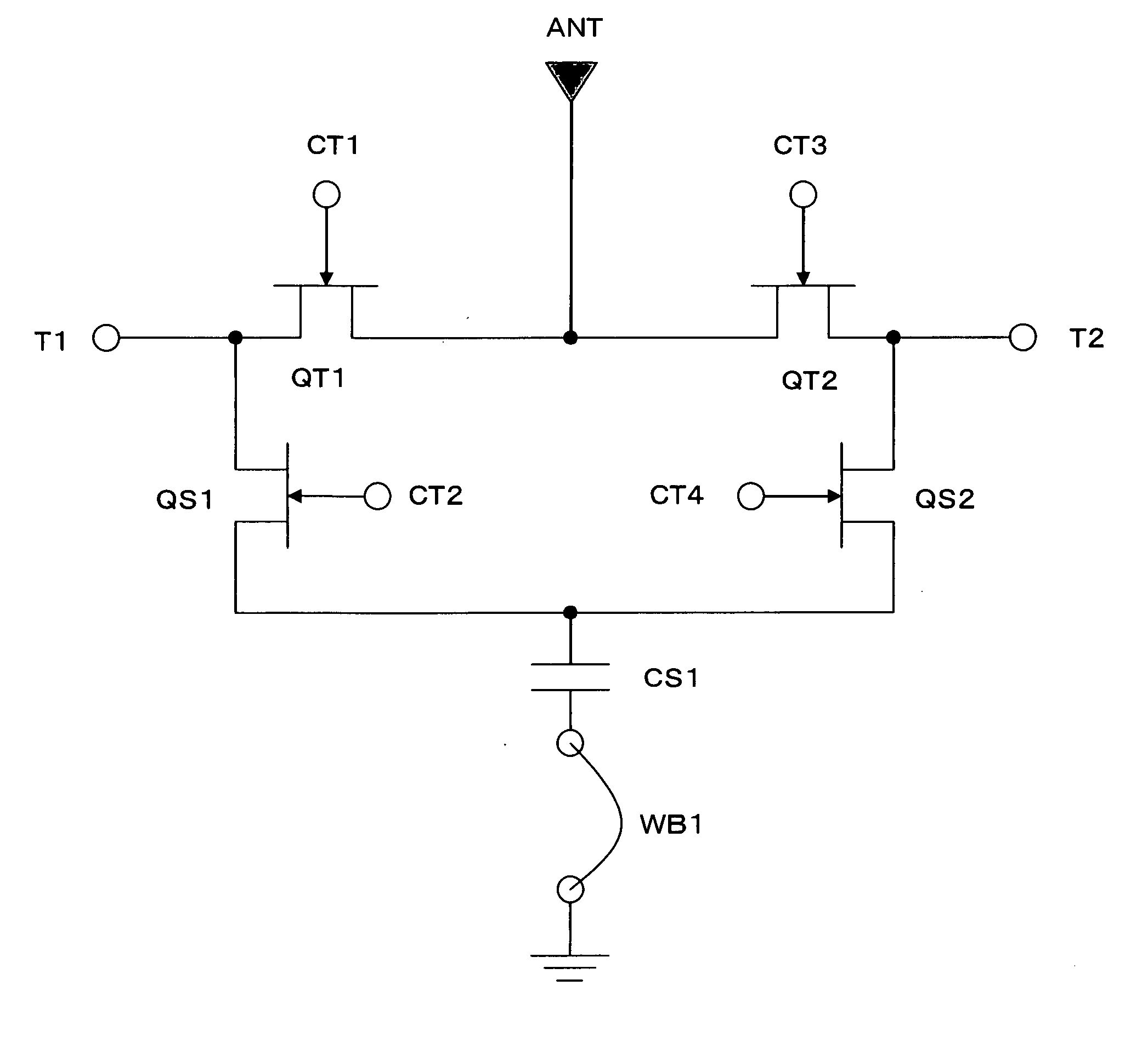
[0049]FIG. 6 is an equivalent circuit diagram illustrating an antenna switch circuit in which a shunt capacitor is commonly used. In FIG. 6, shunt-side field effect transistors QS1 and QS2 are connected to an upper electrode (i.e., one end) of the single shunt capacitor CS1. A lower electrode of the shunt capacitor CS1 (i.e., the other end) is grounded.

[0050] Supposing that the shunt capacitor CS1 of the related art has the capacitance C and the shunt capacitor CS1 of this embodiment has the capacitance C′. When C=C′ is established, a signal inputted via a high frequency signal input / output terminal T1 passes through the upper electrode of the common shunt capacitor CS1 and is leaked to a high frequency signal input / output terminal T2. This deteriorates an isolation characteristic when compared to the related art. Thus, a ground side of the shunt capacitor CS1 must have a lower impedance.

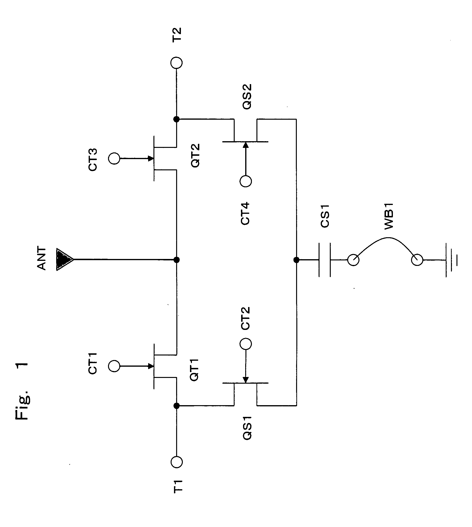
[0051]FIG. 1 is a circuit diagram illustrating a configuration of a first embodiment of the an...

second embodiment

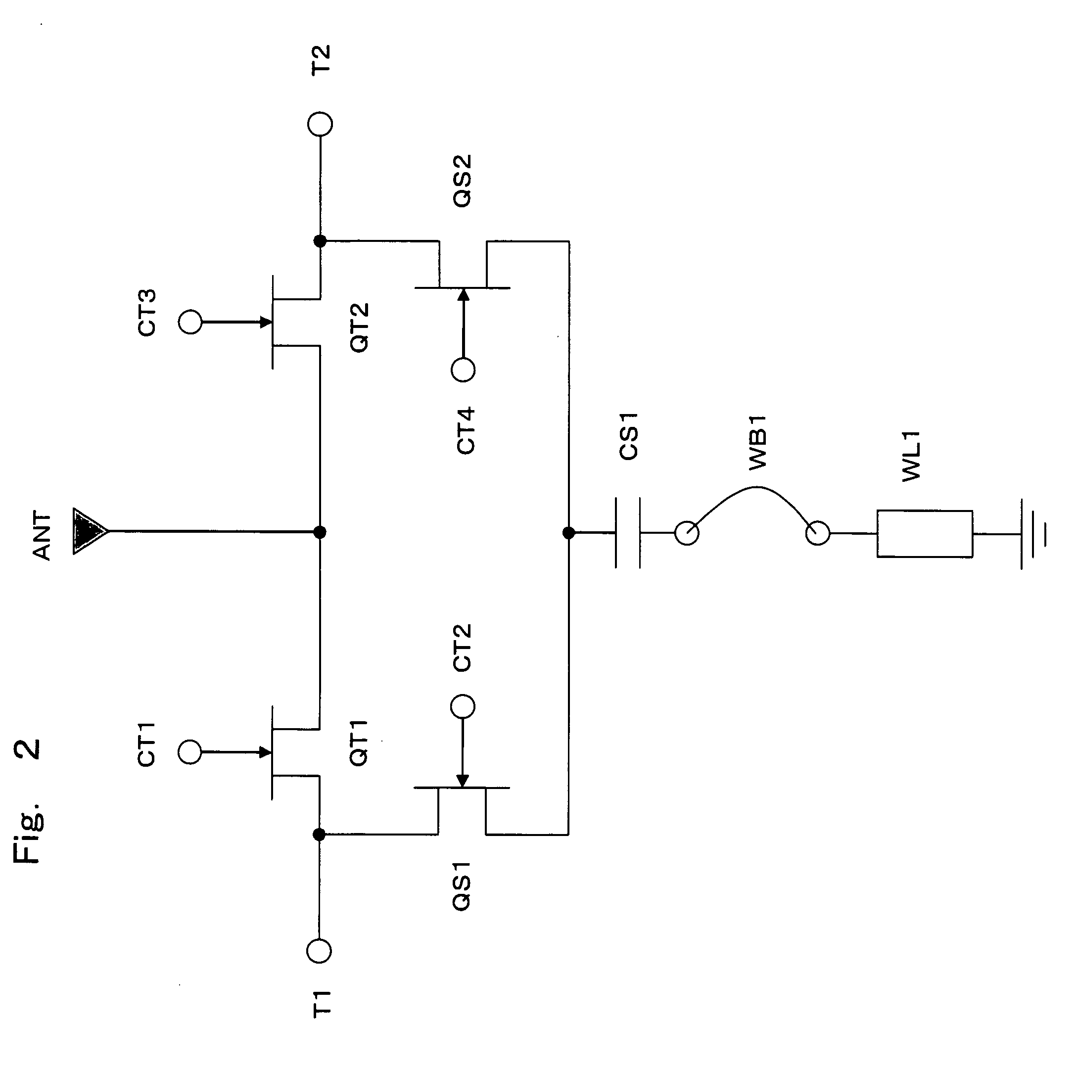
[0060]FIG. 2 is a circuit diagram illustrating a configuration of a second embodiment of an antenna switch circuit according to the present invention. In FIG. 2, the shunt-side field effect transistors QS1 and QS2 are connected to the upper electrode of the single shunt capacitor CS1 and are grounded via the shunt capacitor CS1, the bonding wire WB1, and a wiring WL1. The bonding wire WB1 and the wiring WL1 can be assumed as an inductor equivalently and thus the shunt capacitor CS1, the bonding wire WB1, and the wiring WL1 configure the series resonant circuit.

[0061] In the antenna switch circuit of this embodiment, at least the shunt-side field effect transistors QS1 and QS2 and the through-side field effect transistors QT1 and QT2 are provided on the GaAs substrate. The shunt capacitor CS1 may be provided on the GaAs substrate or may also be provided in the lamination substrate of the Low Temperature Co-fired Ceramics (LTCC). Alternatively, the shunt capacitor CS1 may also be pro...

third embodiment

[0072]FIG. 3 is a circuit diagram illustrating a configuration of a third embodiment of an antenna switch circuit according to the present invention. In this embodiment, the two series resonant circuits described in the first and the second embodiments are arranged in parallel. Specifically, the shunt-side field effect transistors QS1 and QS2 are grounded via two series resonant circuits SR1 and SR2 connected in parallel. Both of the above two series resonant circuits SR1 and SR2 have attenuation poles set at 2 GHz.

[0073] These two series resonant circuits SR1 and SR2 can be provided with the same constant value, thereby securing the isolation across a wide band. As a result, the high isolation characteristic can be realized, for example in both of a GSM band (900 MHz), and a PCS band (1900 MHz) or a DCS band (1800 MHz). Specifically, by providing the two series resonant circuits SR1 and SR2 having the same attenuation pole in parallel, the bandwidth of the pole widens, thereby sec...


PUM


Abstract

First and second through-side field effect transistors are connected between first and second high frequency signal input/output terminals, and an antenna, respectively. The first and the second high frequency signal input/output terminals are connected with one end of the first and the second shunt-side field effect transistors, respectively. A series resonant circuit including a shunt capacitor and a bonding wire is connected between the other end of the first and the second shunt-side field effect transistors, and a ground.

Description

BACKGROUND OF THE INVENTION [0001] 1. Field of the Invention [0002] The present invention relates to an antenna switch circuit, and a composite high frequency part and a mobile communication device using the same. [0003] 2. Description of Related Art [0004] A communication system of a mobile phone includes various modes, such as a GSM (Global System for Mobile Communications) mode and a DCS (Digital Cellular System) mode mainly used in Europe, and a PCS (Personal Communication Service) mode mainly used in North America. [0005] In order to allow a user to use a mobile phone in various regions in the world, the user must carry a required number of mobile phones compatible with the respective modes or must carry one multiband phone compatible with a plurality of communication systems. In the latter case, in order to allow one mobile phone to provide communication through a plurality of communication systems, the phone may be configured by using components of the respective communicatio...

Claims


Application Information

Patent Timeline
Patent Type & Authority Applications(United States)
IPC IPC(8): H03K17/693H01P1/15H01Q3/24H04B1/40
CPCH01P1/15A46B13/06A47L11/185A47L11/19
Inventor SUWA, ATSUSHINAKATSUKA, TADAYOSHI
Owner PANASONIC CORP
Why Eureka
Try Eureka