General purpose pin mapping for a general purpose application specific integrated circuit (ASIC)

a technology of integrated circuits and pin mapping, applied in the field of office automation products, can solve the problems of limited physical connection number, mechanical device handling and package size, and the inability to meet the requirements of pcb (printed circuit board) fabrication,

Active Publication Date: 2005-10-20
SYNAPTICS INC
View PDF10 Cites 8 Cited by
  • Summary
  • Abstract
  • Description
  • Claims
  • Application Information

AI Technical Summary

Benefits of technology

[0021] To overcome the foregoing limitations in prior art chip design, including the problems of pin shortages and selective overrides, the present invention provides a novel way to determine the function of the chip's pins.

Problems solved by technology

More particularly, although silicon gate densities have increased dramatically over the years, following the now-famous Moore's Law, integrated circuit packaging has not developed at the same pace.
Among other things, limitations of PCB (Printed Circuit Board) fabrication, mechanical device handling and package size combine to limit the number of physical connections (“pins”) which it is economically viable to provide between the silicon die and the external system.
The constraints over pin resources are particularly difficult to resolve in a general purpose SoC ASIC component, i.e., a general purpose component which can subsequently be custom configured to perform one or more specific functions.
For a more general purpose SoC ASIC component, however, the required connections cannot be determined in advance, since it is not yet clear what the specific functions of the general purpose ASIC chip will be, so it is necessary to allow the individual pin connections to be assigned at a later time.
The chip itself, however, typically only provides P usable pins (see also FIG. 1).
Given the substantial fixed costs associated with producing each unique chip, it is generally not desirable to develop many similar but different chips.
This complex system of overrides, even when simplified as described above, can be difficult for a firmware developer to program correctly.
Even when it is programmed correctly, overrides can result in unexpected behavior and unnecessary, poorly structured code changes.
A problem with this approach is that one firmware code module must be changed in accordance with the operation of an unrelated firmware code module.
Although this can be done, it violates widely-accepted principles of structured design.

Method used


Image

  • General purpose pin mapping for a general purpose application specific integrated circuit (ASIC)
  • General purpose pin mapping for a general purpose application specific integrated circuit (ASIC)
  • General purpose pin mapping for a general purpose application specific integrated circuit (ASIC)

Examples


Embodiment Construction

Overview

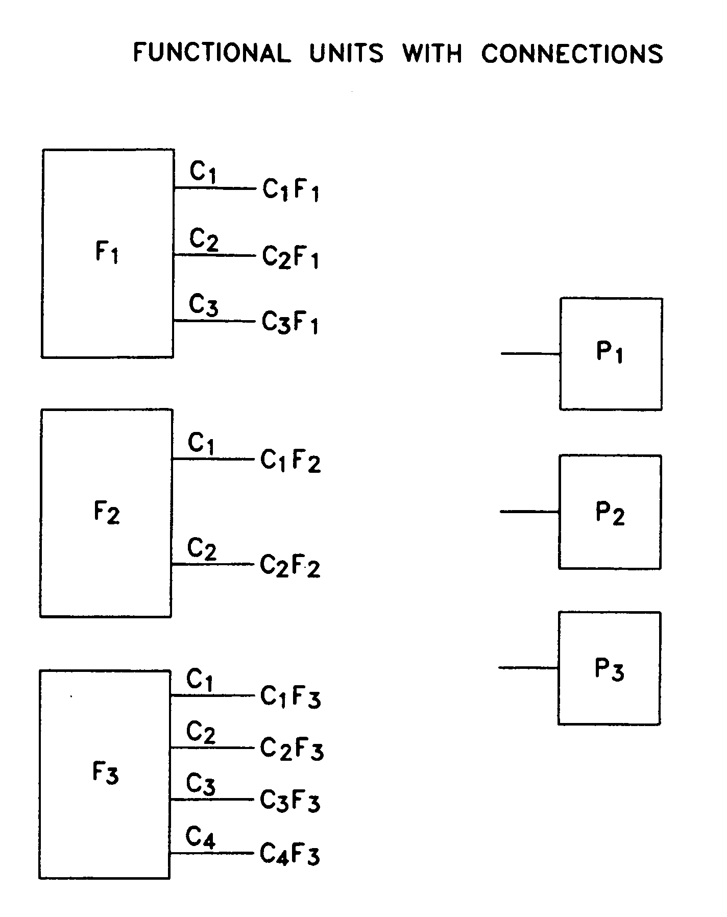
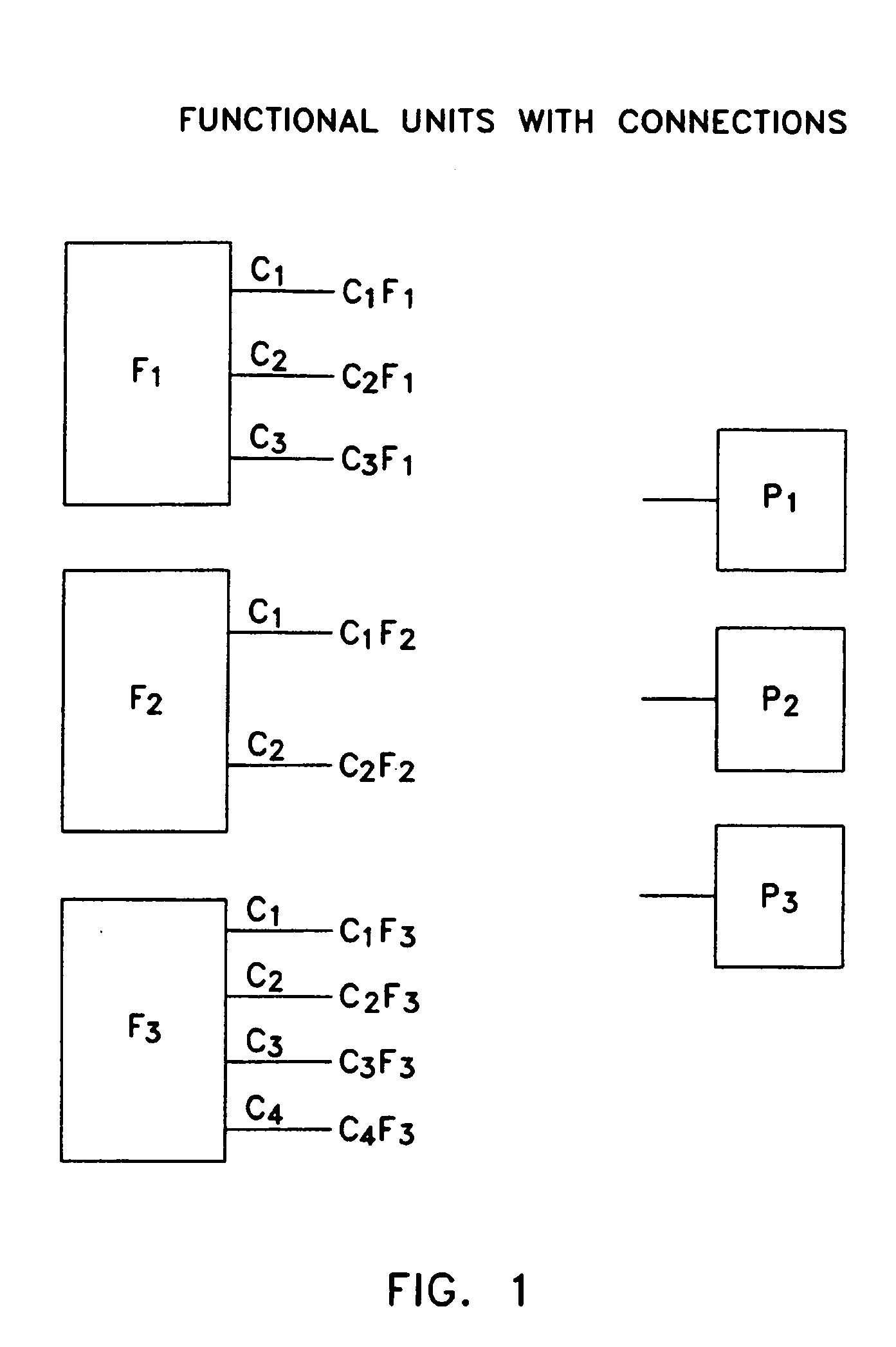
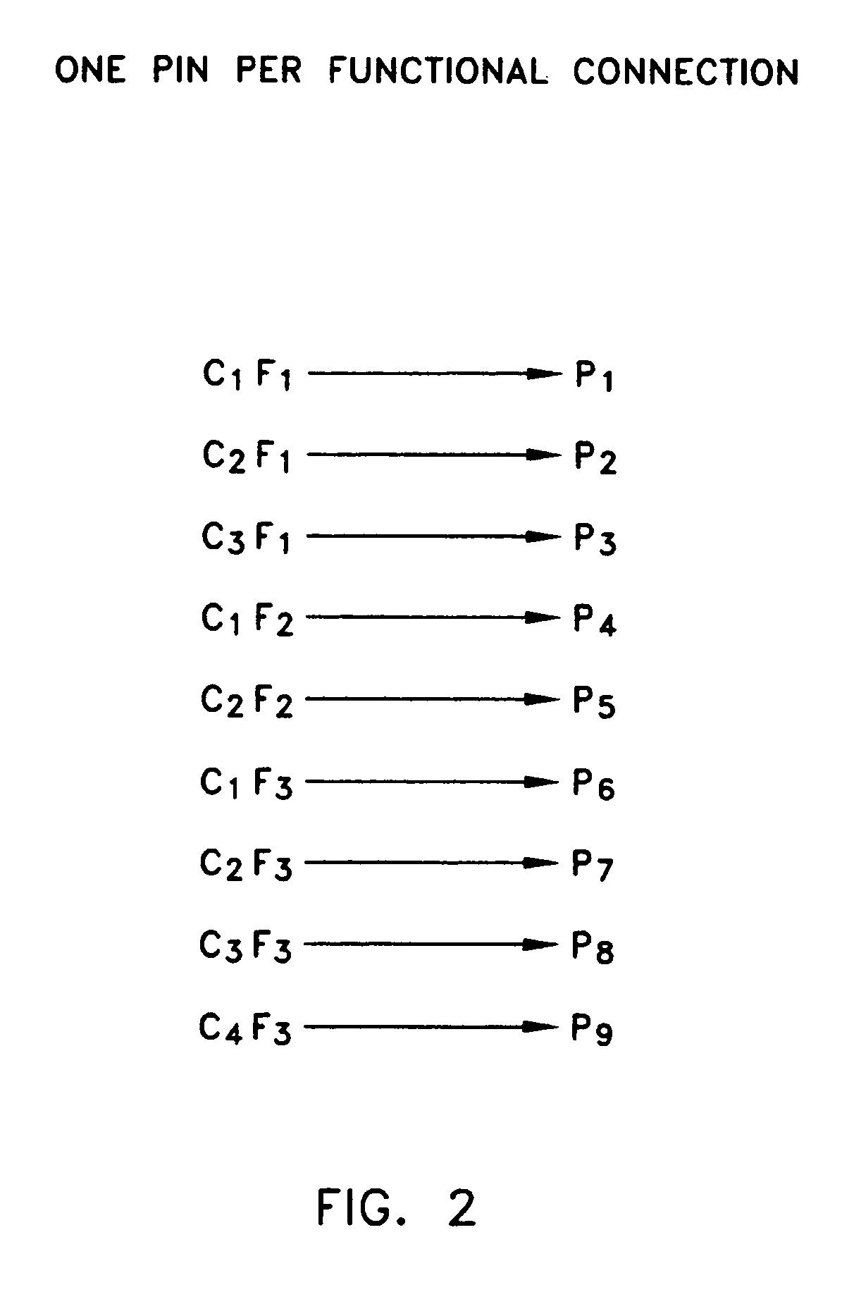
[0050] In one preferred form of the present invention, each pin P of the chip is programmable so as to enable it to be connected with any of the C connections of functional units F (see FIG. 4).

[0051] There are many possible ways to achieve these programmable interconnections. By way of example but not limitation, the programmable interconnections may be effected through the use of a large multiplexer, a crossbar switch, or another internal bus structure. In this way, any functional unit connection CXFY can be provided through any pin PI. Therefore, when the SoC ASIC system is configured during chip preparation by one of many possible means (such as, but not limited to, boot firmware, hardware jumpers, or non-volatile programming registers), each pin PI is assigned a specific functional unit connection CXFY. The benefit of such a configuration is that the functional units are not connected to the pins in a pre-determined manner. Instead, the pins are selectively connectabl...


PUM


Abstract

In one form of the invention, there is provided a general purpose ASIC comprising: a plurality of functional units each having a plurality of connections; a plurality of pins; and an interface for connecting selected connections of selected functional units to selected pins. In another form of the invention, there is provided a method for configuring a general purpose ASIC comprising: providing a general purpose ASIC comprising: a plurality of functional units each having a plurality of connections; a plurality of pins; and an interface for connecting selected connections of selected functional units to selected pins; and configuring said interface so as to connect selected connections of selected functional units to selected pins.

Description

REFERENCE TO PENDING PRIOR PATENT APPLICATION [0001] This patent application claims benefit of pending prior U.S. Provisional Patent Application Ser. No. 60 / 535,228, filed Jan. 09, 2004 by Derek T. Walton et al. for GENERAL PURPOSE PIN MAPPING (Attorney's Docket No. OASIS-1 PROV). [0002] The above-identified patent application is hereby incorporated herein by reference.FIELD OF THE INVENTION [0003] This invention relates to office automation products in general, and more particularly to printers, fax machines, scanners, copiers and the like. Even more particularly, this invention relates to the integration of formerly separate functions into single devices such as those sometimes referred to as MFPs (Multi-Functional-Peripherals), and the integration of multiple functions into a single ASIC (Application Specific Integrated Circuit) such as those produced by Oasis Semiconductor, Inc. of Waltham, Mass. BACKGROUND OF THE INVENTION The Problem of Limited Pin Connections [0004] When desi...

Claims


Application Information

Patent Timeline
Patent Type & Authority Applications(United States)
IPC IPC(8): G06F1/22H04Q11/00
CPCG06F1/22
Inventor WALTON, DEREK T.MIKKELSEN, CARL M.SCHAFFSTEIN, MICHAEL J.DEMATTIA, ROBERT J.
Owner SYNAPTICS INC
Why Eureka
Try Eureka