Transparent contact for light emitting diode

a technology of light-emitting diodes and transparent contacts, which is applied in the direction of basic electric elements, electrical apparatus, and semiconductor devices, can solve the problems of ohmic contact with a low scr, and is rather difficult to achieve ohmic contact with a low scr, and achieves the effect of enhancing transparent conta

Inactive Publication Date: 2005-10-27
ARIMA COMP
View PDF3 Cites 17 Cited by
  • Summary
  • Abstract
  • Description
  • Claims
  • Application Information

AI Technical Summary

Benefits of technology

[0008] It is therefore an objective of the present invention to provide a enhanced transparent contact for gallium nitride-based light emitting diodes.

Problems solved by technology

These devices require electrodes with low specific contact resistance (SCR) for current injection and thus considerable effort has been devoted to developing low resistance contacts for GaN.
Because of the low carrier concentration and high work function of p-GaN, it is rather more difficult to achieve an ohmic contact with a low SCR.

Method used


Image

  • Transparent contact for light emitting diode
  • Transparent contact for light emitting diode
  • Transparent contact for light emitting diode

Examples


Embodiment Construction

[0020] Reference will now be made in detail to the present preferred embodiments of the invention, examples of which are illustrated in the accompanying drawings. Wherever possible, the same reference numbers are used in the drawings and the description to refer to the same or like parts.

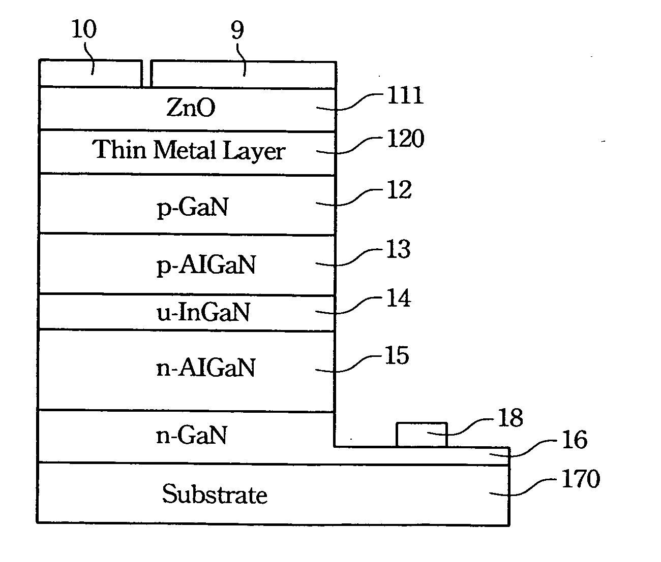
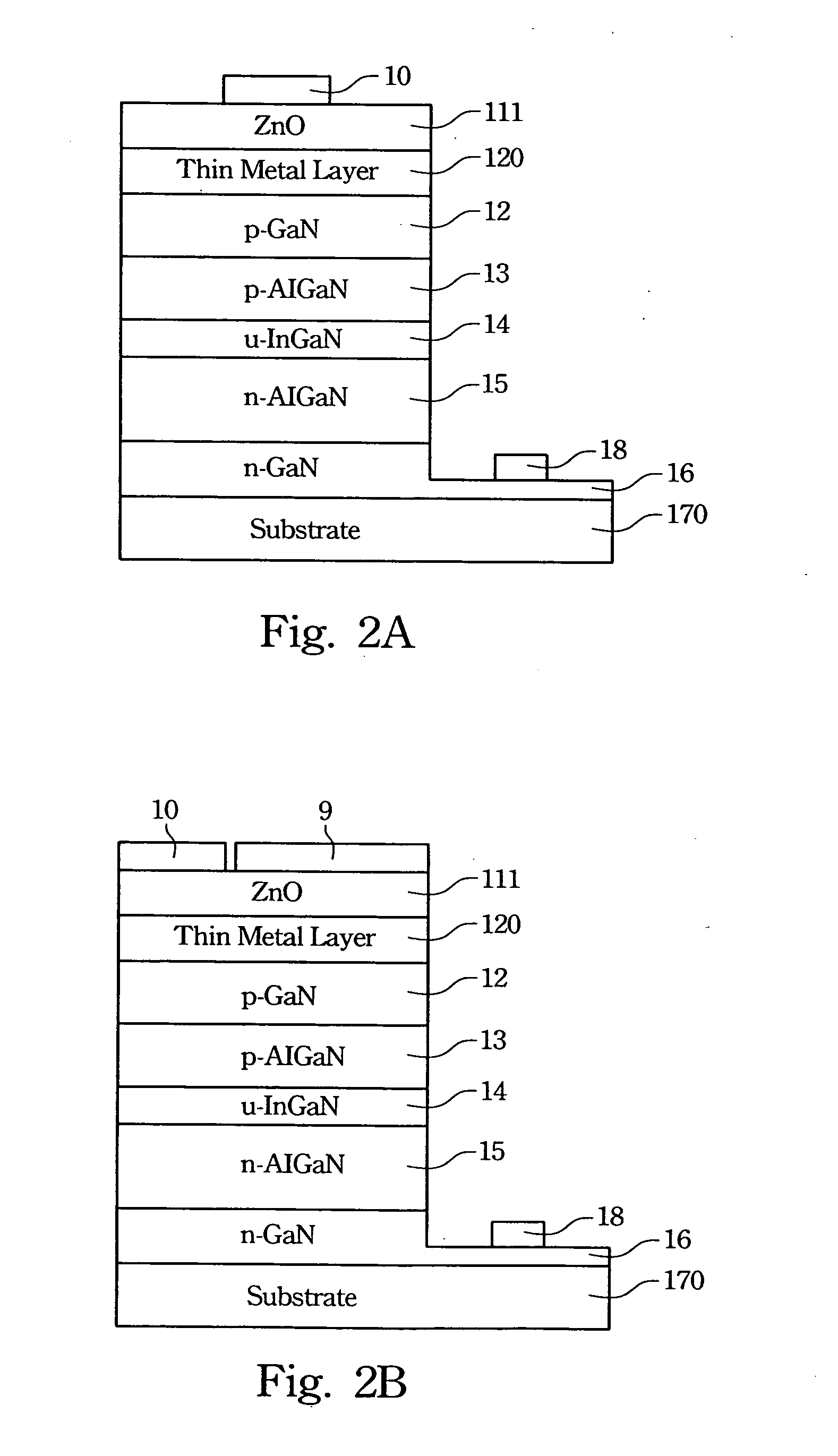
[0021] In order to spread the current evenly, reduce the series resistance and increase light transmittance at certain wavelength, a transparent conductive film is deposited between a semiconductor diode and its electrode. Zinc Oxide (ZnO) can be used as the transparent conductive film, which is particularly applicable to a GaN-based light emitting diode.

[0022]FIG. 2A illustrates a light emitting diode design with a ZnO transparent contact according to one preferred embodiment of this invention. A transparent insulating material, including sapphire (Al2O3), lithium-gallium oxide (LiAlO2), lithium-aluminum oxide (LiGaO2), and spinal (MgAl2O4), serves as a substrate 170. A buffer layer (n-GaN) 16, a...


PUM


Abstract

A transparent conductive film is deposited between the electrode and semiconductor diode to spread the current evenly, reduce the series resistance and increase light transmittance at certain wavelength. ZnO film can be used as the transparent conductive film. The Ni/Au/ZnO film is found to have an increased light transmission compared with an annealed Ni/Au contact. The maximum optical transmission measured through the Ni/Au/ZnO film is 90%.

Description

BACKGROUND [0001] 1. Field of Invention [0002] The present invention relates to a transparent contact for light emitting diodes. More particularly, the present invention relates to a transparent contact for gallium nitride-based light emitting diodes. [0003] 2. Description of Related Art [0004] In recent years, GaN-based semiconductors have become increasingly attractive as material for high power optoelectronic devices in the blue and violet region of the visible spectrum. These devices require electrodes with low specific contact resistance (SCR) for current injection and thus considerable effort has been devoted to developing low resistance contacts for GaN. For surface emitting devices, another important consideration is the optical transparency of the contact, at the wavelength of the emitted radiation. [0005] Many reports demonstrate low SCR for contacts on n-GaN using metal or Si implantation of the GaN. The reports also indicate the existence of fewer problems in achieving a...

Claims


Application Information

Patent Timeline
Patent Type & Authority Applications(United States)
IPC IPC(8): H01L27/15H01L31/12H01L33/32H01L33/42
CPCH01L33/42H01L33/32
Inventor WANG, WANG-NANG
Owner ARIMA COMP
Why Eureka
Try Eureka