Super trench MOSFET including buried source electrode and method of fabricating the same

a source electrode and super-torque technology, applied in the field of trench gated metaloxidesilicon field-effect transistors (mosfets) and diodes, can solve problems such as errors, and achieve the effect of reducing gate-to-drain capacitance and resistivity of drift region when the device is turned

Inactive Publication Date: 2005-11-03
SILICONIX
View PDF15 Cites 80 Cited by
  • Summary
  • Abstract
  • Description
  • Claims
  • Application Information

AI Technical Summary

Benefits of technology

[0013] The buried source electrode is electrically connected to the source region. As a result, when the MOSFET is reverse-biased, the source electrode depletes the drift region in a direction transverse to the general direction of current flow. There is normally a similar trench on the opposite side of the drift region, so the drift region is depleted from both sides. This allows the doping concentration of the drift region to be significantly higher than it would otherwise need to be to block a reverse current flow between the drain and the source. Therefore, the resistivity of the drift region is far less when the device is turned on.
[0014] In addition, the buried source electrode separates the gate from the drain and thereby reduces the gate-to-drain capacitance, allowing the MOSFET to operate at high frequencies.

Problems solved by technology

There is a vertical overlap between the buried source electrode and the gate electrode which provides a margin of error in the diffusion of the body region.

Method used


Image

  • Super trench MOSFET including buried source electrode and method of fabricating the same
  • Super trench MOSFET including buried source electrode and method of fabricating the same
  • Super trench MOSFET including buried source electrode and method of fabricating the same

Examples


Embodiment Construction

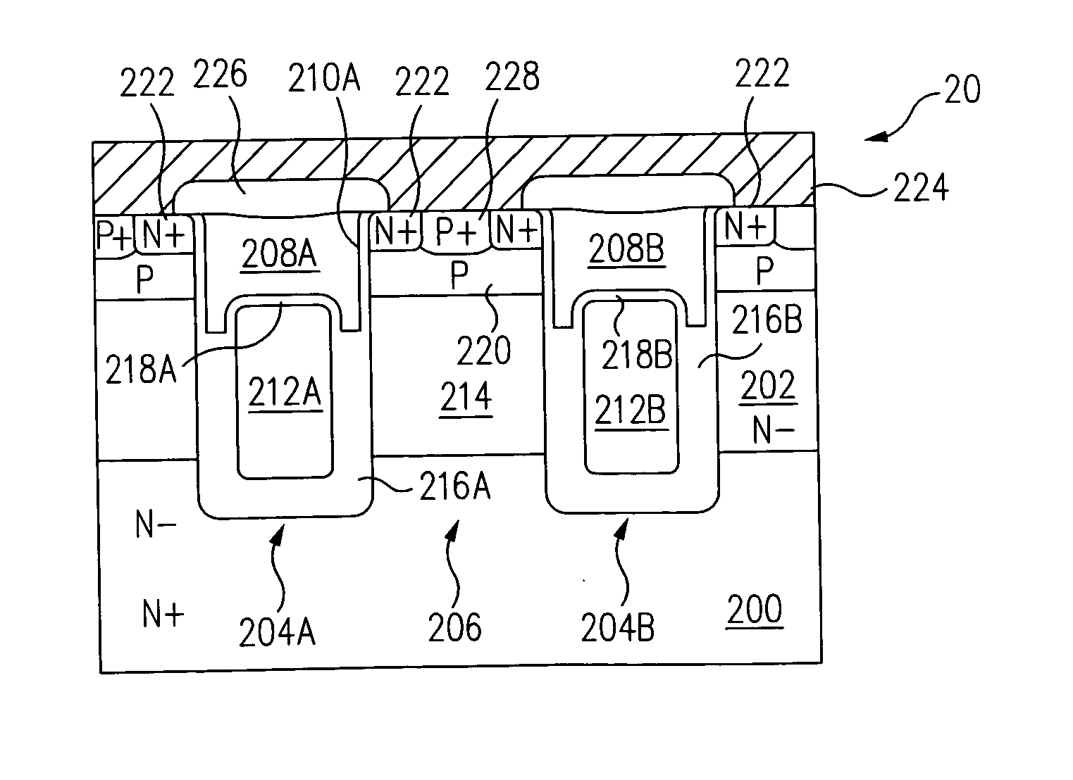
[0034]FIG. 2 illustrates a cross-sectional view of an N-channel MOSFET 20 in accordance with this invention. MOSFET 20 is formed in an epitaxial (epi) layer 202 that is grown on an N+ substrate 200. Trenches 204A and 204B and are formed in epi layer 202. Trenches 204A and 204B are separated by a mesa 206. While FIG. 2 shows only two trenches, it will be understood by those of skill in the art that the trenches and mesas shown in FIG. 2 typically represent only a tiny fraction of the total number of trenches and mesas in the actual device, which may number in the millions. The trenches and mesas may be arranged in a variety of geometric patterns on the surface of epi layer 202. In some of the most common of these patterns, the mesas are hexagons, squares or longitudinal stripes and are separated by trenches of uniform width and depth. As trenches 204A and 204B are identical, only trench 204A will be described in detail. It will be understood that the structure of trench 204B is ident...


PUM


Abstract

In a trench MOSFET, the lower portion of the trench contains a buried source electrode, which is insulated from the epitaxial layer and semiconductor substrate but in electrical contact with the source region. When the MOSFET is in an “off” condition, the bias of the buried source electrode causes the “drift” region of the mesa to become depleted, enhancing the ability of the MOSFET to block current. The doping concentration of the drift region can therefore be increased, reducing the on-resistance of the MOSFET. The buried source electrode also reduces the gate-to-drain capacitance of the MOSFET, improving the ability of the MOSFET to operate at high frequencies. The substrate may advantageously include a plurality of annular trenches separated by annular mesas and a gate metal layer that extends outward from a central region in a plurality of gate metal legs separated by source metal regions.

Description

FIELD OF THE INVENTION [0001] This invention relates to semiconductor devices that include a gate electrode formed in a trench, and in particular to trench-gated metal-oxide-silicon field-effect transistors (MOSFETs) and diodes. BACKGROUND OF THE INVENTION [0002] Power MOSFETs are the preferred switching devices for notebook computers and other portable electronic devices, and they are also widely used for switching currents in the automotive industry. In a common form of MOSFET, the gate electrode is formed in a trench that extends downward from the surface of the chip, and current flows primarily in a vertical direction between a source region on one surface of the chip and a drain region on the other surface of the chip. The source region is normally shown on the top surface of the chip and the drain region is shown on the bottom surface of the chip, although this orientation is arbitrary. The trench is lined with a dielectric layer (typically silicon dioxide), and a channel is f...

Claims


Application Information

Patent Timeline
Patent Type & Authority Applications(United States)
IPC IPC(8): H01L21/336H01L29/06H01L29/40H01L29/417H01L29/423H01L29/78
CPCH01L29/0696H01L29/407H01L29/41741H01L29/4236H01L29/7813H01L29/42376H01L29/4238H01L29/66734H01L29/42368H01L29/7811H01L29/063
Inventor PATTANAYAK, DEVA N.BAI, YUMINGTERRILL, KYLEYUE, CHRISTIANAXU, ROBERTLUI, KAM HONGCHEN, KUO-INSHI, SHARON
Owner SILICONIX
Why Eureka
Try Eureka