Self-aligned copper silicide formation for improved adhesion/electromigration

a technology of self-aligned copper silicide and adhesion/electromigration, which is applied in the direction of semiconductor devices, semiconductor/solid-state device details, electrical devices, etc., can solve the problems of not providing sufficient coverage or uniformity, and not providing the required adhesion strength for the terminal layer

Inactive Publication Date: 2004-11-16
GLOBALFOUNDRIES INC
View PDF14 Cites 3 Cited by
  • Summary
  • Abstract
  • Description
  • Claims
  • Application Information

AI Technical Summary

Benefits of technology

The invention reduces such delamination by forming the silicide layer over the last metalization layer to generally at least 10-20% the thickness of the LM layer. This extensive silicide formation is required at the LM level to resolve the copper / nitrite adhesion issues discussed above. Also, because the last metalization layer comprises very thick metallurgy, it is substantially less sensitive to resistivity shifts and therefore, the resistivity problems noted with conventional copper silicide (CuSi) systems is avoided. The improved surface coverage provided by the invention enables less resistivity shift per percent thickness of LM layer formation.

Problems solved by technology

However, Filipiak's method is limited specifically it does not provide sufficient coverage or uniformity and, consequently, it does not provide the required adhesion strength for the terminal layer to remain connected to the last metalization (LM) layer.

Method used


Image

  • Self-aligned copper silicide formation for improved adhesion/electromigration
  • Self-aligned copper silicide formation for improved adhesion/electromigration

Examples


Embodiment Construction

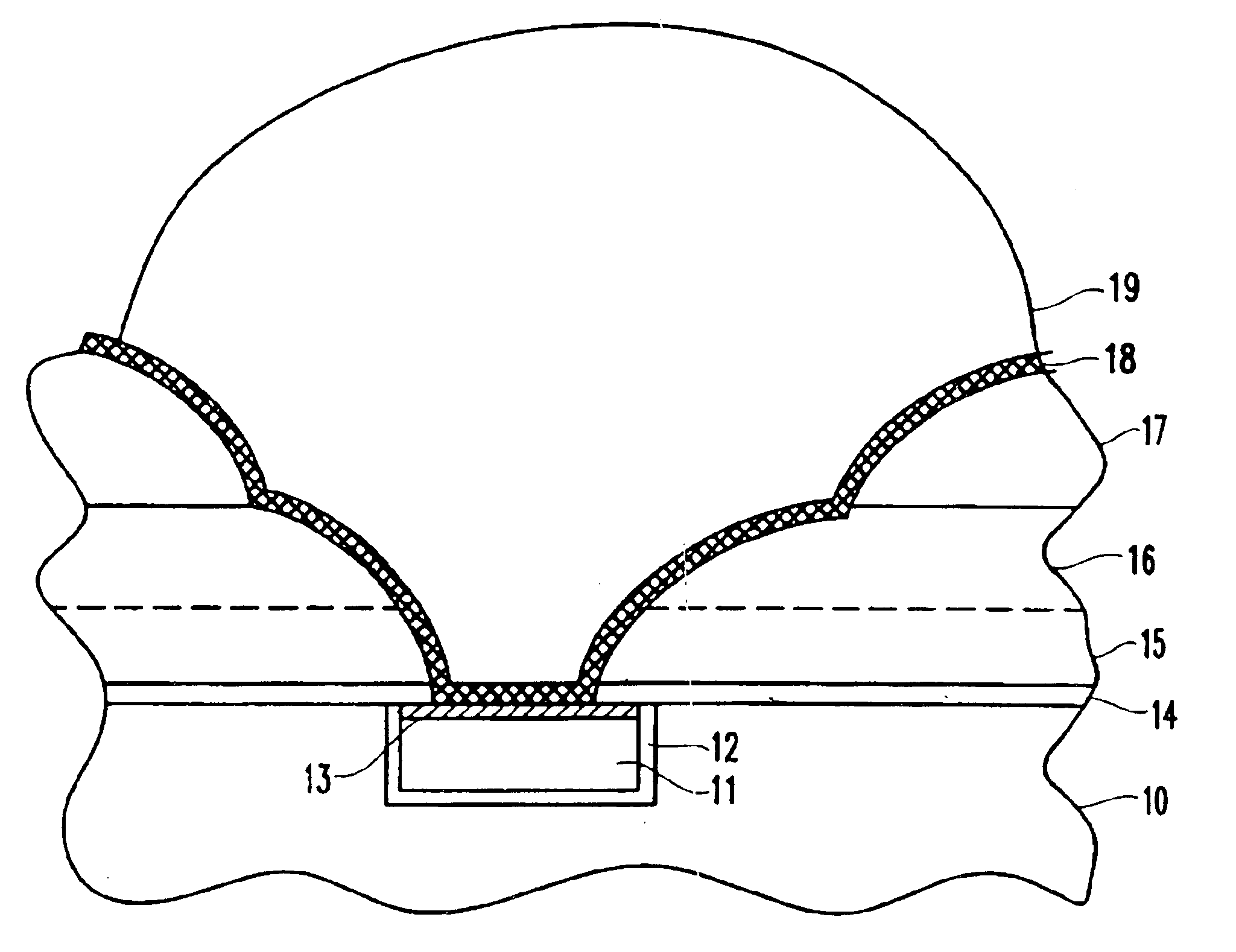
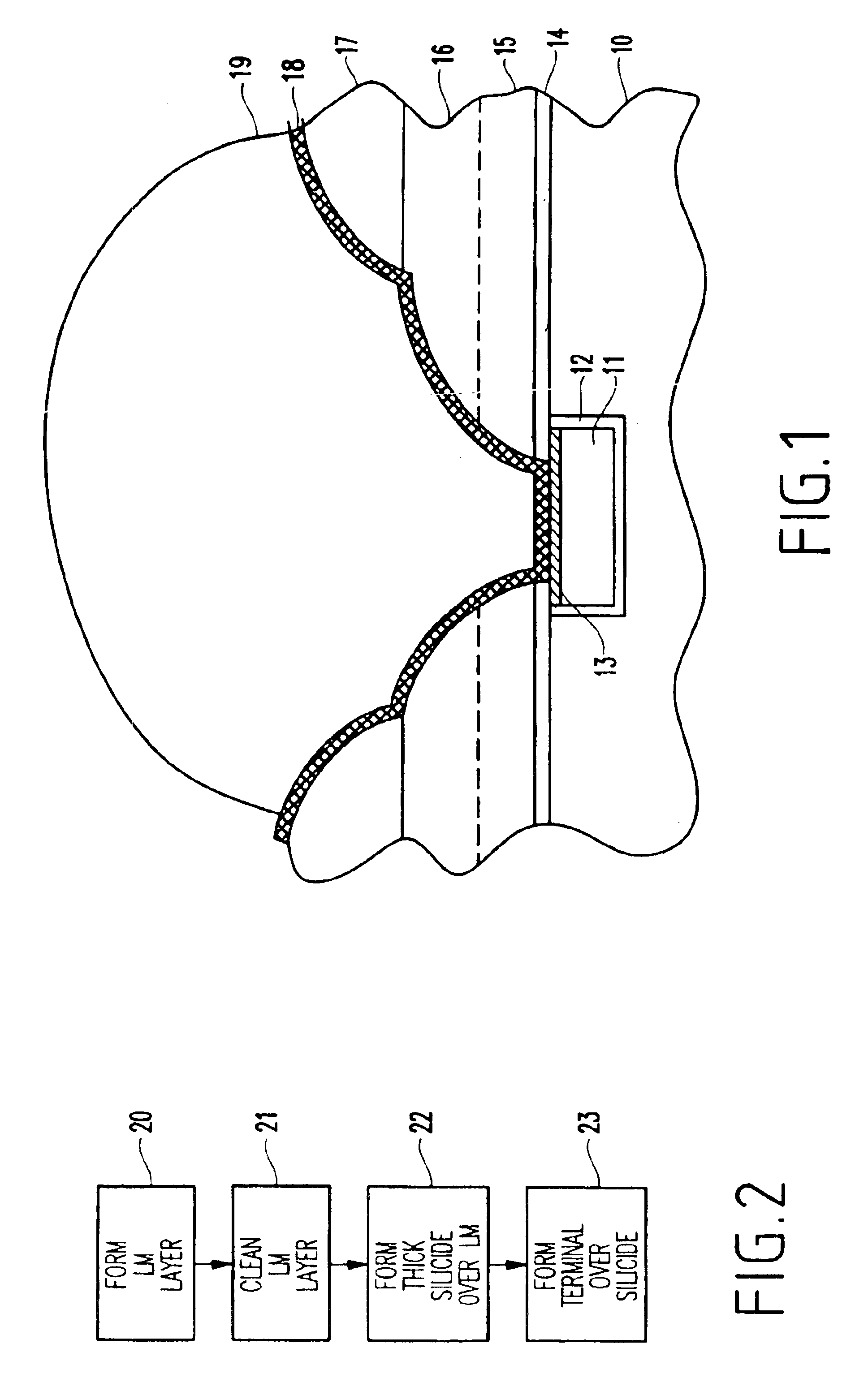
As described above, the conventional methods for improving adhesion between interior copper wiring layers and adjacent insulating layers do not provide sufficient reliability of the terminal layer (e.g., the C4 layer) over the last metalization (LM) layer. The invention solves this problem by cleaning the exposed copper wiring layer and increasing the thickness of the silicide layer above 10%.

Special problems exist with the adhesion of the last metalization layer because the last metalization layer is subject to higher levels and different forms of stress than are the other metalization lawyers within the structure. For example, the last metalization is often physically connected to a solder ball terminal layer which is used to make electrical and physical contact to exterior structures. The exterior structure moves differently (through physical movement) and may have different thermal coefficients of expansion which tends to place high levels of stress (including shearing forces) o...


PUM


Abstract

A method for forming a semiconductor structure includes supplying a structure having an exposed last metalization layer, cleaning the last metalization layer, forming a silicide in a top portion of the last metalization layer and forming a terminal over the silicide.

Description

1. Field of the InventionThe present invention generally relates to methods for increasing the adhesion of a terminal to the top copper wiring level in semiconductor devices.2. Description of the Related ArtConventional systems have improved the adhesion of silicon nitride to an interior copper wiring surface by the addition of an intervening copper silicide layer. For example, as described in U.S. Pat. No. 5,447,887 to Filipiak et al., hereinafter "Filipiak" (incorporated herein by reference), the connections of internal levels within a semiconductor device are improved with an intervening copper silicide layer.The silicide layer is conventionally formed within a plasma enhanced chemical vapor deposition (PECVD) reaction chamber by introducing silane (SiH.sub.4) in the absence of a plasma into the chamber. The silane reacts with exposed copper surfaces to form copper silicide. After a sufficient thickness of copper silicide is formed, plasma is generated and gases are introduced in...

Claims


Application Information

Patent Timeline
Patent Type & Authority Patents(United States)
IPC IPC(8): H01L21/60H01L21/02H01L21/3065H01L21/3205H01L21/302H01L21/44H01L21/768H01L23/52
CPCH01L21/76849H01L21/76883H01L24/11H01L21/76867H01L2924/014H01L2224/13099H01L2924/01004H01L2924/01013H01L2924/01029H01L2924/01051H01L2924/01073H01L2924/01074H01L2924/01082H01L2924/04953H01L2924/19042H01L2924/01006H01L2924/01033H01L2224/05001H01L2224/05022H01L2224/05556H01L2224/05572H01L24/03H01L24/05H01L24/13H01L21/44
Inventor ARMBRUST, DOUGLAS S.GIBSON, MARGARET L.SERIANNI, LAURAWHITE, ERIC J.
Owner GLOBALFOUNDRIES INC
Why Eureka
Try Eureka