Organic electro-luminescence device and fabrication method thereof

a technology of electroluminescence device and organic material, which is applied in the direction of discharge tube/lamp details, discharge tube luminescnet screen, organic semiconductor device, etc., can solve the problems of large display size, large weight and slimming, and limited entire process yield, so as to reduce the design margin of tfts on the lower substra

Active Publication Date: 2005-11-03
LG DISPLAY CO LTD
View PDF3 Cites 28 Cited by
  • Summary
  • Abstract
  • Description
  • Claims
  • Application Information

AI Technical Summary

Benefits of technology

[0021] An advantage of the present invention is to provide an organic electro-luminescence device and method of fabricating same wherein corresponding pixel regions of first and second substrates are not aligned accurately. Instead, they are misaligned by position of the conductive spacers designed on each substrate and then attached to each other. In this manner, the position of the conductive spacer is set free, such that design margin of the TFTs on the lower substrate can be reduced.
[0022] Additional features and advantages of the invention will be set forth in the description which follows, and in part will become apparent from the description, or may be learned by practice of the invention. The objective and other advantages of the invention may be realized and attained by the structure particularly pointed out in the written description and claims hereof as well as the appended drawings.
[0023] To achieve these objective and other advantages and in accordance with the purpose of the invention, as embodied and broadly described herein, there is provided an organic electro-luminescence device first and second substrates spaced a predetermined distance apart from each other, sub-pixels being defined in the substrates; an array element having at least one thin film transistor (TFT) formed on an inner surface of the first substrate in each sub-pixel unit; a conductive spacer electrically connected to a drive TFT of the array element; a first electrode for an organic electro-luminescence diode disposed on an inner surface of the second substrate; and an organic electro-luminescence layer and a second electrode for the organic electro-luminescence diode, which are sequentially formed on the first electrode in each sub-pixel unit, wherein the first substrate and the second substrate are misaligned by a predetermined distance and attached to each other, such that the conductive spacer is in contact with a conductive spacer contact region provided on the second electrode.
[0024] In another aspect of the present invention, there is provided a method of fabricating an organic electro-luminescence device, the method comprising: forming an array element having at least one TFT formed on an inner surface of a first substrate in a sub-pixel unit; forming a conductive spacer electrically connected to a drive TFT of the array element; forming a first electrode for an organic electro-luminescence diode on an inner surface of a second substrate; sequentially forming an organic electro-luminescence layer and a second electrode for the organic electro-luminescence diode on the first electrode in the sub-pixel unit; and misaligning the first and second substrates by a predetermined distance and attaching the first and second substrates, such that the conductive spacer is in contact with a conductive spacer contact region provided on the second electrode.
[0025] It is to be understood that both the foregoing general description and the following detailed description of the present invention are exemplary and explanatory and are intended to provide further explanation of the invention as claimed.

Problems solved by technology

However, the LCD is a non-luminous display device and has technical limitations with regard to brightness, contrast, viewing angle, and large display size.
Also, since the organic electro-luminescence device does not require a backlight assembly, it is lightweight and slim.
Therefore, the entire process yield is greatly restricted by the late process, that is, the process of forming the organic electro-luminescence diode.
For example, even though excellent array elements are formed, if foreign particles or other factors cause defects in forming the organic electro-luminescence layer using a thin film of about 1000 Å thick, the corresponding organic electro-luminescence device is a defective grade.
Thus, there occurs loss of every expense and material cost spent in fabricating the non-defective array element, resulting in yield reduction.
In addition, the bottom emission type organic electro-luminescence device has high stability and high degree of freedom due to the encapsulation, but has limitation in aperture ratio.
Thus, the bottom emission type organic electro-luminescence device is difficult to apply to high-definition products.
However, since the cathode is disposed on the organic electro-luminescence layer, the selection of material is restricted.
Consequently, the transmittance is limited and the luminous efficiency is degraded.

Method used


Image

  • Organic electro-luminescence device and fabrication method thereof
  • Organic electro-luminescence device and fabrication method thereof
  • Organic electro-luminescence device and fabrication method thereof

Examples


Embodiment Construction

[0035] Reference will now be made in detail to embodiments of the present invention, examples of which are illustrated in the accompanying drawings. Wherever possible, the same reference numbers will be used throughout the drawings to refer to the same or like parts.

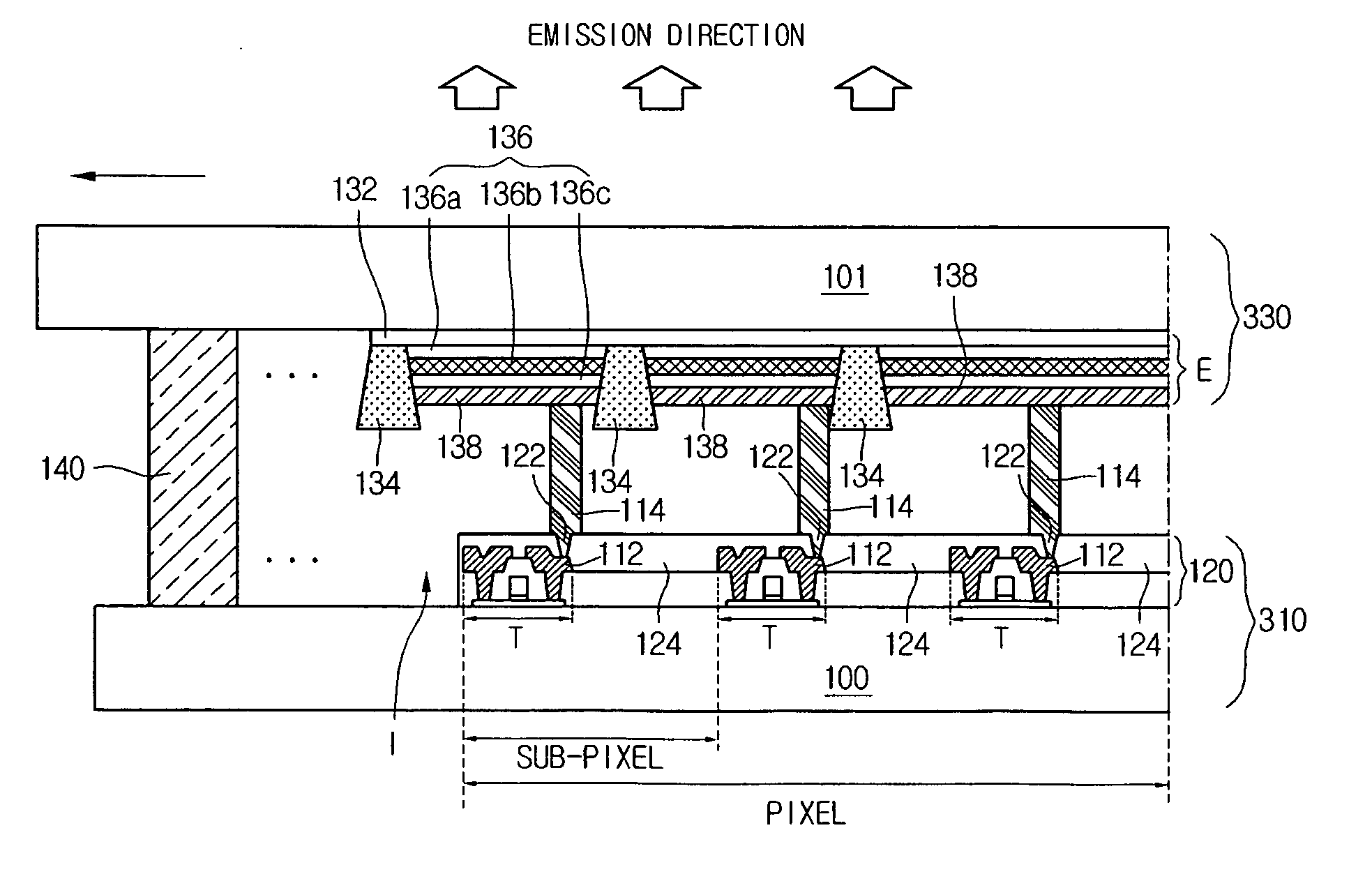
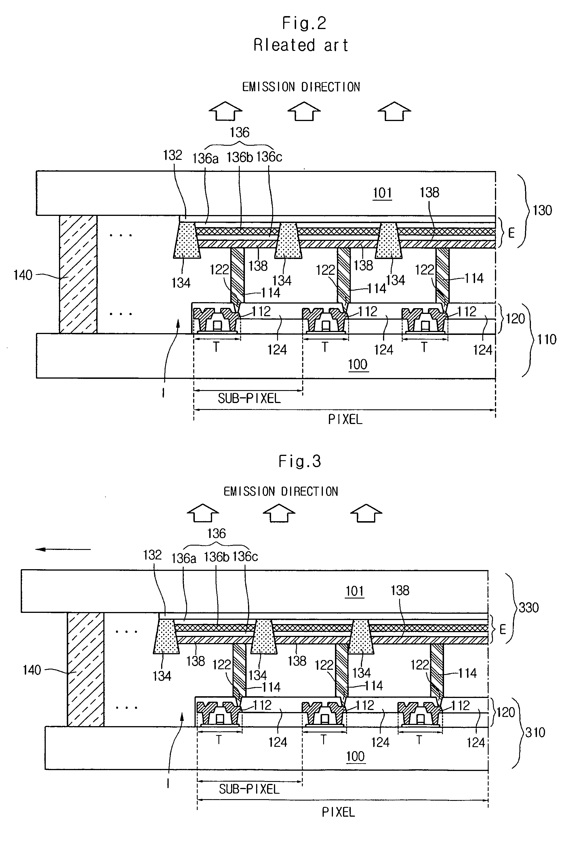
[0036]FIG. 2 is a schematic view of section of a dual panel type organic electro-luminescence device. For the convenience of explanation, only one pixel region is illustrated in the drawing. Referring to FIG. 2, first and second substrates 110 and 130 are arranged spaced apart from each other by a predetermined distance. An organic electro-luminescence diode E is formed on an inner surface of a transparent substrate 101 of the second substrate 130. Edges of the first and second substrates 110 and 130 are encapsulated by a seal pattern 140.

[0037] The organic electro-luminescence diode E includes a first electrode 132 used, for example, as a common electrode, an electrode separator 134 disposed at a sub-pixel boundary be...


PUM


Abstract

An organic electro-luminescence device is provided. First and second substrates are arranged spaced apart from each other by a predetermined distance and sub-pixels are defined in the substrates. An array element has at least one thin film transistor (TFT) formed on an inner surface of the first substrate in sub-pixel unit. A conductive spacer is electrically connected to a drive TFT of the array element. A first electrode for an organic electro-luminescence diode is disposed on an inner surface of the second substrate. An organic electro-luminescence layer and a second electrode for the organic electro-luminescence diode are sequentially formed on the first electrode in sub-pixel unit. The first substrate and the second substrate are misaligned by a predetermined position and attached to each other, such that the conductive spacer is in contact with a conductive spacer contact region provided on the second electrode.

Description

[0001] This application claims the benefit of Korean Patent Application No. 30382, filed on Apr. 30, 2004, which is hereby incorporated by reference for all purposes as if fully set forth herein. BACKGROUND OF THE INVENTION [0002] 1. Field of the Invention [0003] The present invention relates to an organic electro-luminescence device, and more particularly, to an organic electro-luminescence device having upper and lower substrates asymmetrically attached to each other and a method fabricating method same. [0004] 2. Description of the Related Art [0005] In the field of flat panel display devices, liquid crystal display devices (LCD) are widely used because of they are lightweight and have low power consumption. However, the LCD is a non-luminous display device and has technical limitations with regard to brightness, contrast, viewing angle, and large display size. Therefore, new flat panel display devices capable of overcoming these drawbacks are actively being developed. [0006] One...

Claims


Application Information

Patent Timeline
Patent Type & Authority Applications(United States)
IPC IPC(8): H01L27/32H05B33/00H05B33/02
CPCH01L2251/5315H01L27/3253H10K59/1275H10K2102/3026H05B33/00
Inventor BAE, SUNG JOONLEE, JAE YOON
Owner LG DISPLAY CO LTD
Why Eureka
Try Eureka