Semiconductor integrated circuit device

a technology of integrated circuits and semiconductors, applied in logic circuits, pulse techniques, instruments, etc., can solve the problems of display data not being loaded normally, display data prevailing immediately after, and fluctuation of the potential of bias wiring

Inactive Publication Date: 2005-11-03
NEC ELECTRONICS CORP
View PDF5 Cites 11 Cited by
  • Summary
  • Abstract
  • Description
  • Claims
  • Application Information

AI Technical Summary

Benefits of technology

[0019] The present invention is such that in a semiconductor integrated circuit device in which data is loaded upon receipt of input of a start signal, the operation of a data receiver can be restored to the steady state at high speed without causing fluctuation of bias potential applied to a clock-signal receiver.

Problems solved by technology

However, in a case where a bias potential is supplied from a bias circuit to the clock-signal and display-data receivers via common bias wiring in this method, a problem which arises is that the potential of the bias wiring fluctuates when the input of the start signal is received and the operation of the display-data receiver restored.
If the speed of the clock signal is raised further at this time, there is the danger that the display data prevailing immediately after the start of loading of the display data will not be loaded normally.

Method used


Image

  • Semiconductor integrated circuit device
  • Semiconductor integrated circuit device
  • Semiconductor integrated circuit device

Examples


first embodiment

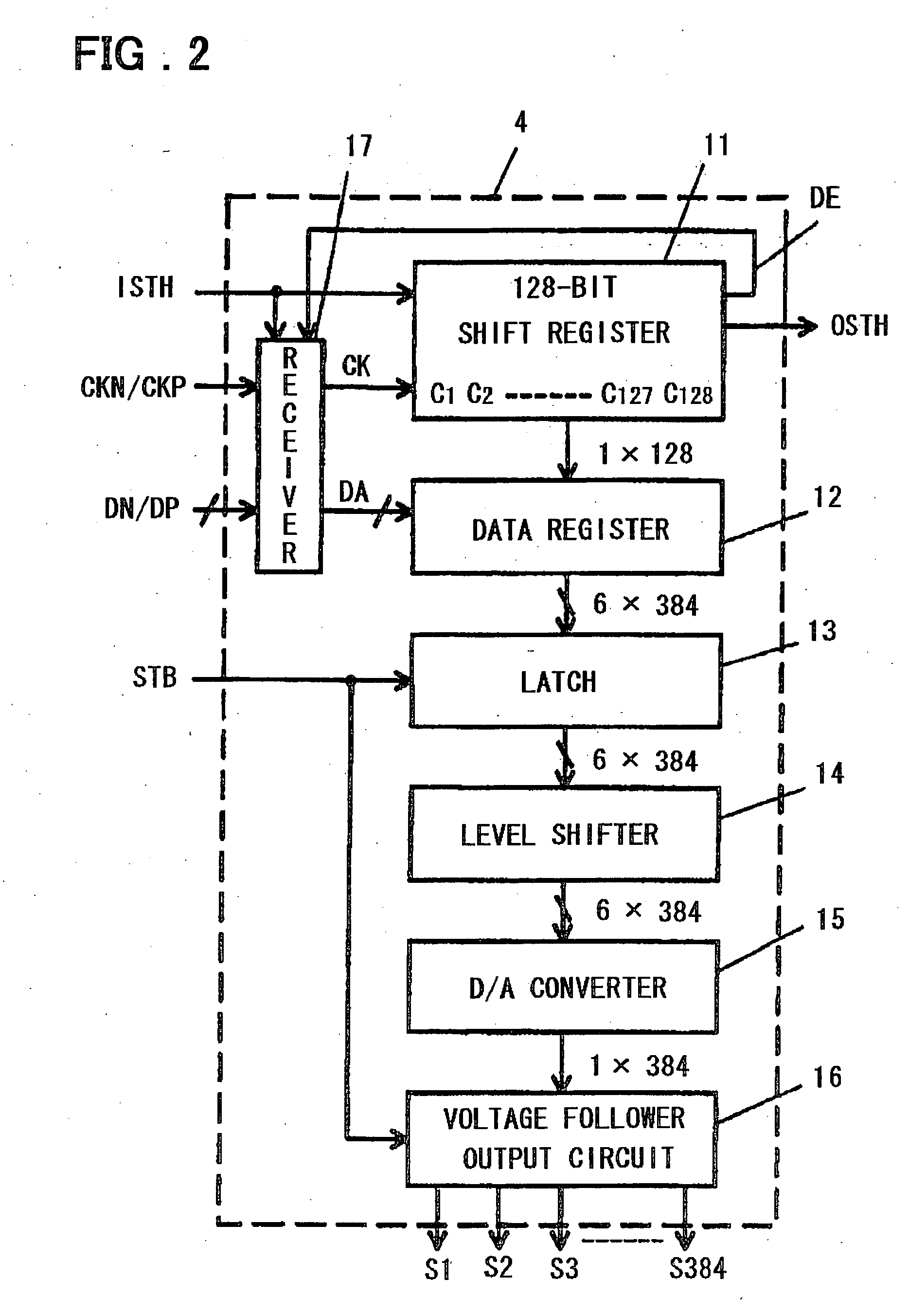
[0053] Reference will be had to FIGS. 3 to 6 to describe a receiver 20 of a first embodiment used as the receiver 17. As shown in FIG. 3, the receiver 20 includes a first receiver 21 for a clock signal; a plurality of second receivers 22 for display data; a control signal generating circuit 23 for generating control signals Vc1, Vc2; a plurality of switches 24 for changing over between supply and cut-off of the bias potential to the second receivers 22 depending upon the control signal Vc1; and a bias circuit 25 for supplying a first bias potential Vb1 to the first receiver 21 and a second bias potential Vb2 to the second receivers 22 to cause the first receiver 21 and second receivers 22 to operate. The first bias potential output Vb1 of the bias circuit 25 is led out by first bias wiring 26, and the second bias potential output Vb2 of the bias circuit 25 is led out by second bias wiring 27. The switches 24 correspond to respective ones of the second receivers 22, and the switches ...

second embodiment

[0067] A receiver 30 used as the receiver 17 will be described next with reference to FIGS. 7 to 9. Components identical with those of the receiver 20 shown in FIG. 3 are designated by like reference characters and need not be described again. The receiver 30 in FIG. 7 differs from the receiver 20 of FIG. 3 in that the receiver 30 has a bias circuit 35 instead of the bias circuit 25. Further, the bias circuit 35 differs from the bias circuit 25 in that it has a second bias potential generating circuit 353 instead of the second bias potential generating circuit 253 and further includes a precharging circuit 354 and precharging power supply 355, as shown in FIG. 8.

[0068] The second bias potential generating circuit 353 has a circuit structure, which is similar to that of the first bias potential generating circuit 252, constituted by MOS transistors Q23, Q24 instead of the MOS transistors Q13, Q14 of the first bias potential generating circuit 252 in order to output a steady bias pot...

third embodiment

[0078] A receiver 40 used as the receiver 17 will be described next with reference to FIGS. 10 to 13. Components identical with those of the receivers 20 and 30 shown in FIGS. 3 and 7 are designated by like reference characters and need not be described again. The receiver 40 in FIG. 10 differs from the receiver 20 of FIG. 3 in that the receiver 40 has a control signal generating circuit 43 instead of the control signal generating circuit 23 and a bias circuit 45 instead of the bias circuit 25, and in that a capacitor 46 is connected between ground and the node of the connection between the second bias wiring 27 and each switch 24. The control signal generating circuit 43 differs from the control signal generating circuit 23 in that it does not have the pulse-width adjusting circuit 232, as illustrated in FIG. 11. Further, the bias circuit 45 differs from the bias circuit 25 in that it has the second bias potential generating circuit 353, which is used in the bias circuit 35 of the...


PUM

PropertyMeasurementUnit
clock frequencyaaaaaaaaaa
bias potentialsaaaaaaaaaa
bias potentialaaaaaaaaaa

Abstract

A semiconductor IC device includes a receiver having a bias circuit that applies a first bias potential to a first receiver for a clock signal and a second bias potential to each of a plurality of receivers for display data. The first bias potential is led out by first bias wiring, the second bias potential is led out by second bias wiring, and switches are connected between the second bias wiring 27 and respective ones the second receivers. The first bias potential is a steady bias potential, and the second bias potential is a high bias potential for a prescribed period of time from turn-on of the switches and becomes a steady bias potential after a prescribed period of time.

Description

FIELD OF THE INVENTION [0001] This invention relates to a semiconductor integrated circuit device and, more particularly, to a semiconductor integrated circuit device the inputs to which are a clock signal and a data signal, which have the format of low-amplitude differential signals. BACKGROUND OF THE INVENTION [0002] By virtue of such advantages as thinness, light weight and low power, liquid crystal display devices are used as dot-matrix-type display devices in equipment such as personal computers. In particular, active-matrix color liquid crystal display devices, which are advantageous in that image quality is controlled to a high definition, now dominate. [0003] The liquid crystal display module of a liquid crystal display device includes a liquid crystal panel (LCD panel), a control circuit (referred to as a “controller” below) comprising a semiconductor integrated circuit device (referred to as an “IC” below), a scanning-side driver circuit (referred to as a “scan driver” bel...

Claims


Application Information

Patent Timeline
Patent Type & Authority Applications(United States)
IPC IPC(8): G02F1/133G09G3/20G09G3/36H03K19/00H03K19/0175
CPCG09G3/2096G09G2330/06G09G2310/027G09G3/3688
Inventor UEDA, TOSHIAKI
Owner NEC ELECTRONICS CORP
Why Eureka
Try Eureka