

Transistor array substrate fabrication for an LCD
- Summary
- Abstract
- Description
- Claims
- Application Information
AI Technical Summary
Benefits of technology
Problems solved by technology
Method used
Image

Examples
Embodiment Construction
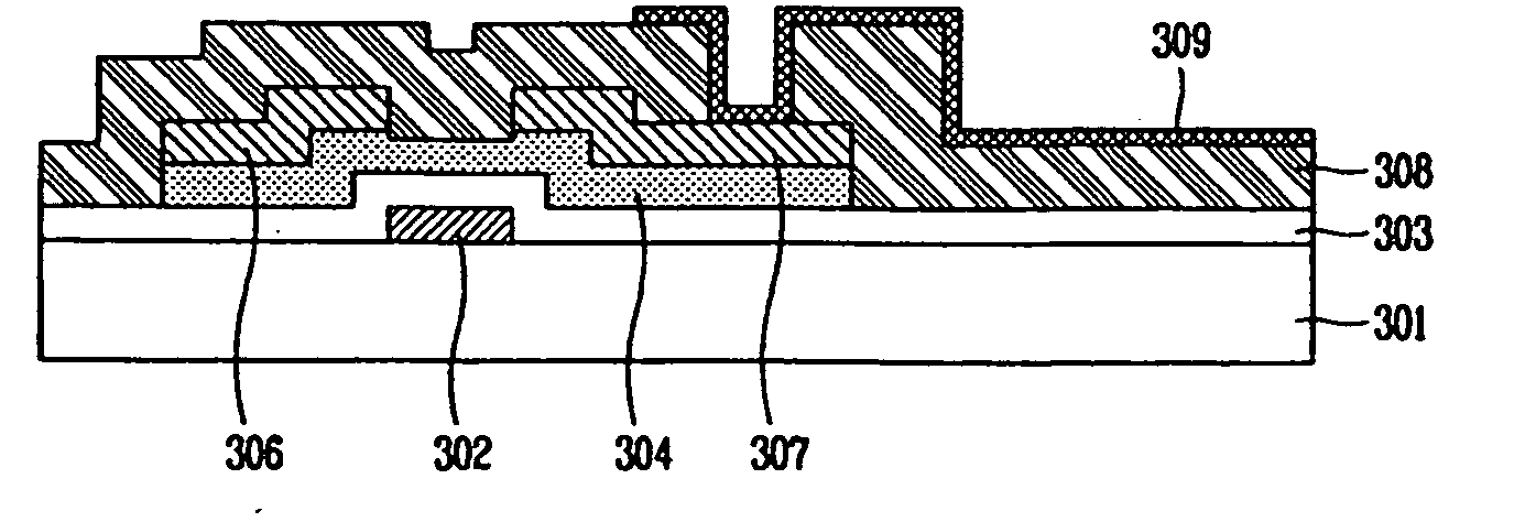
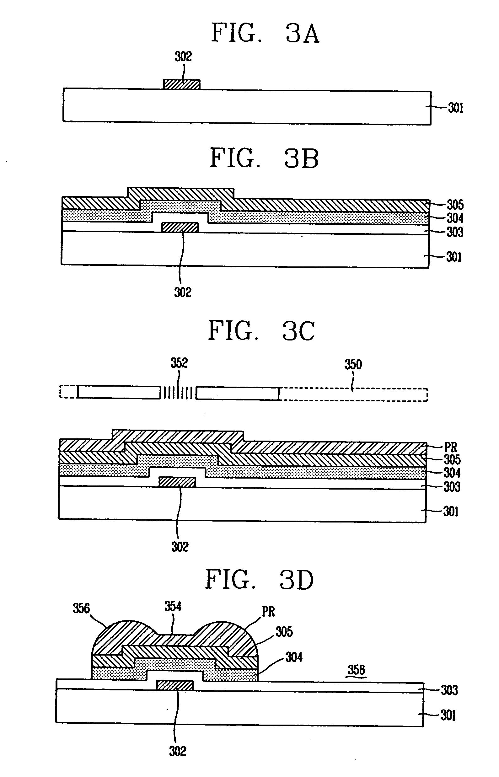
[0030] Reference will now be made in detail to an exemplary implementation of the present invention, illustrated in the accompanying drawings. As will be explained in more detail below, array substrates areas of various sizes are selected for a common glass substrate, and then TFT array substrates are formed in those areas in order to fabricate various models of LCD panels using the same TFT fabrication process for each TFT array substrate.
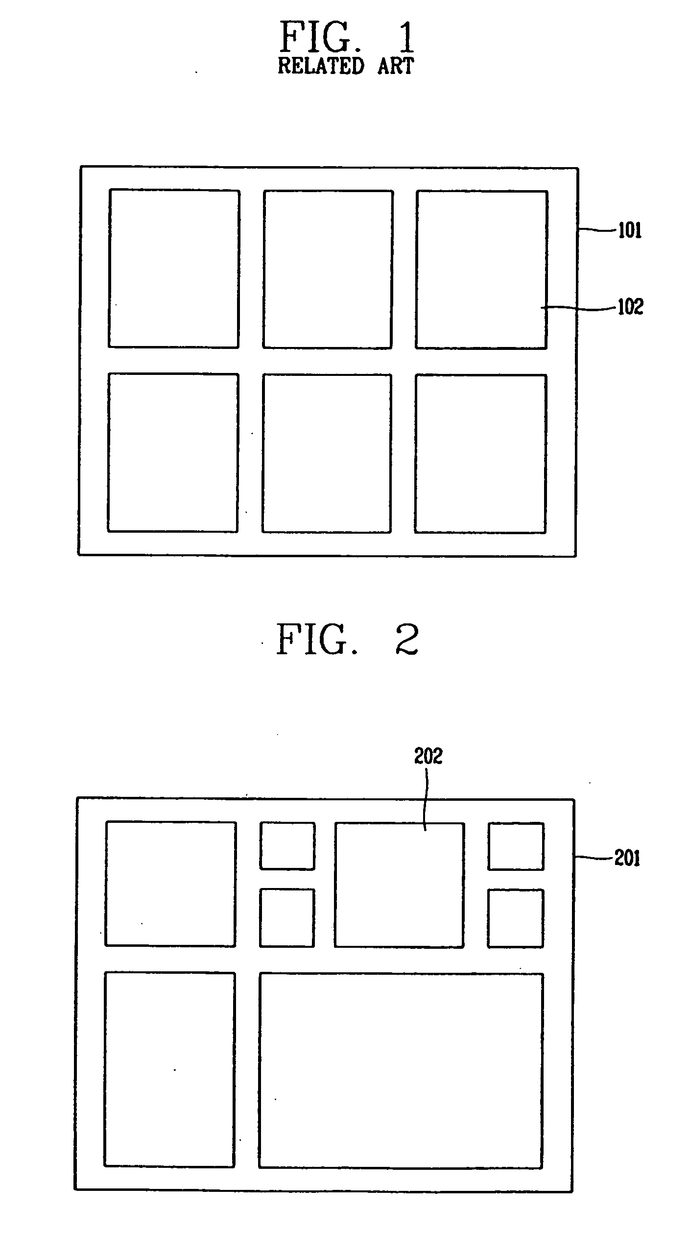
[0031]FIG. 2 shows TFT array substrates 202 of various sizes disposed on a common glass substrate 201 that will yield LCD panels of various sizes when fabrication is complete. Initially, the area that each TFT array substrate 202 will occupy is decided and assigned to the common glass substrate 201, followed by the fabrication steps that create the TFT array substrates.
[0032] In one implementation, the TFT array substrates 202 are arranged on the glass substrate 201 by arranging the TFT array substrates 202 along straight lines to allow effectiv...
PUM
 Abstract
Description
Claims
Application Information