Single line bayer RGB bad pixel correction

a pixel correction circuit and single-line technology, applied in the field of single-line bayer rgb bad pixel correction circuits, can solve the problems of complex continuous maintenance of such maps, high cost of permanent storage of defective pixels in additional memory devices, and the inability to detect defective pixels “on the fly” , to achieve the effect of low cost and effective detection of defective pixels

Inactive Publication Date: 2005-11-10
DIALOG IMAGING SYST
View PDF6 Cites 85 Cited by
  • Summary
  • Abstract
  • Description
  • Claims
  • Application Information

AI Technical Summary

Benefits of technology

[0011] The herewith disclosed invention provides a mechanism to effectively detect defective pixels “on the fly” in a Bayer RGB type color image sensor. The presented invention is primarily intended to and is optimized for low cost applications. It calculates a variable threshold

Problems solved by technology

Permanently storing the manufactures “bad pixel map” in an additional memory device is expensive and continuously maintaining such map is complex.
Evaluatin

Method used


Image

  • Single line bayer RGB bad pixel correction
  • Single line bayer RGB bad pixel correction
  • Single line bayer RGB bad pixel correction

Examples


Embodiment Construction

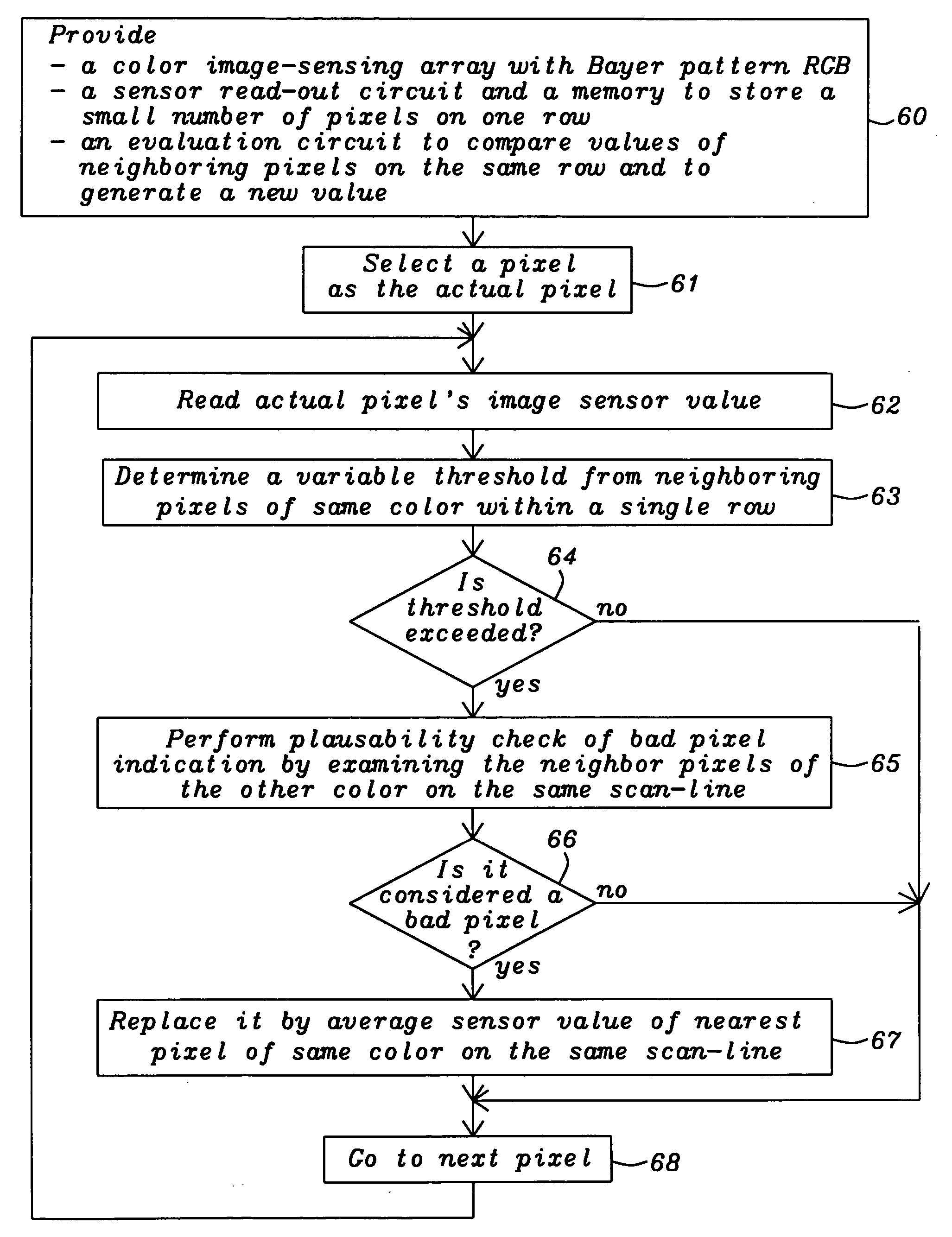
[0022] The objectives of this invention are to perform an effective bad pixel correction in a low cost application.

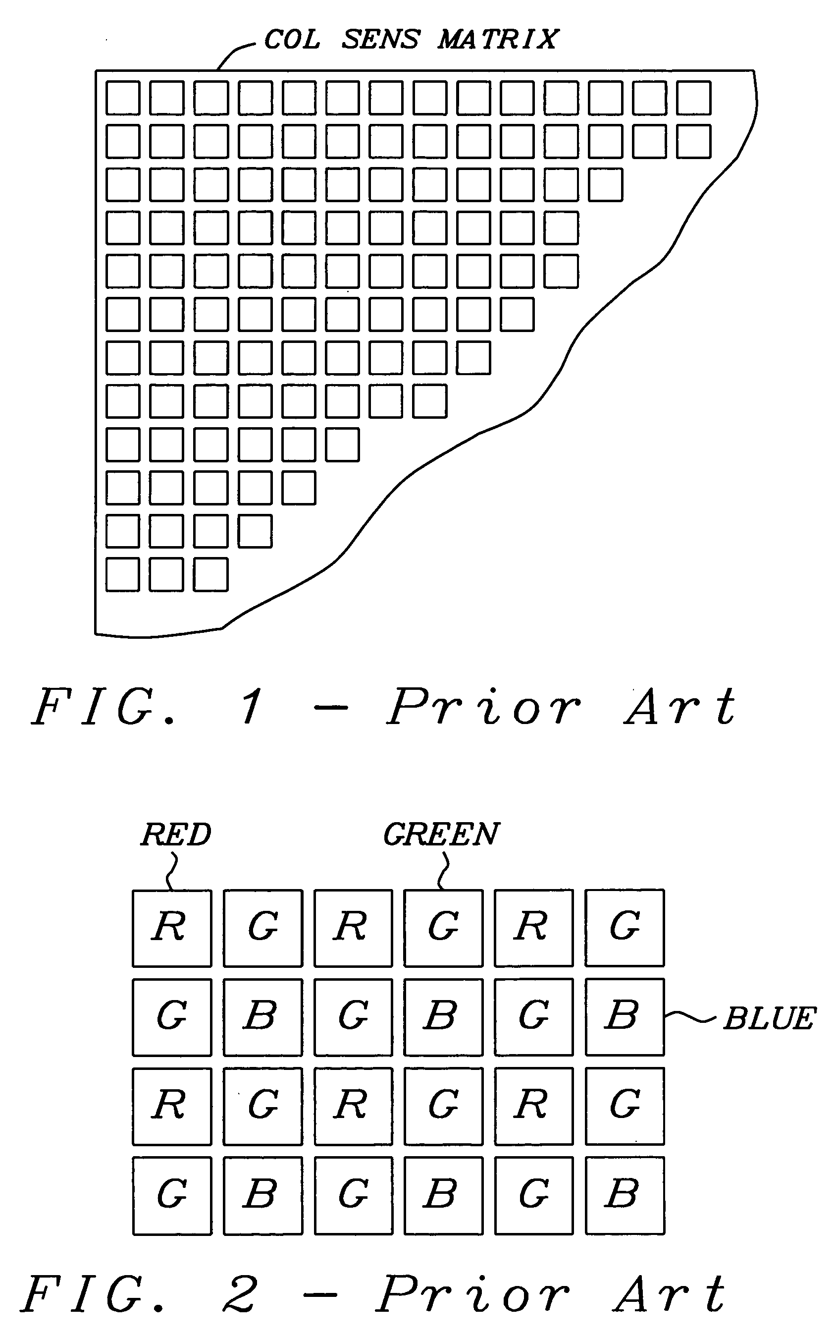
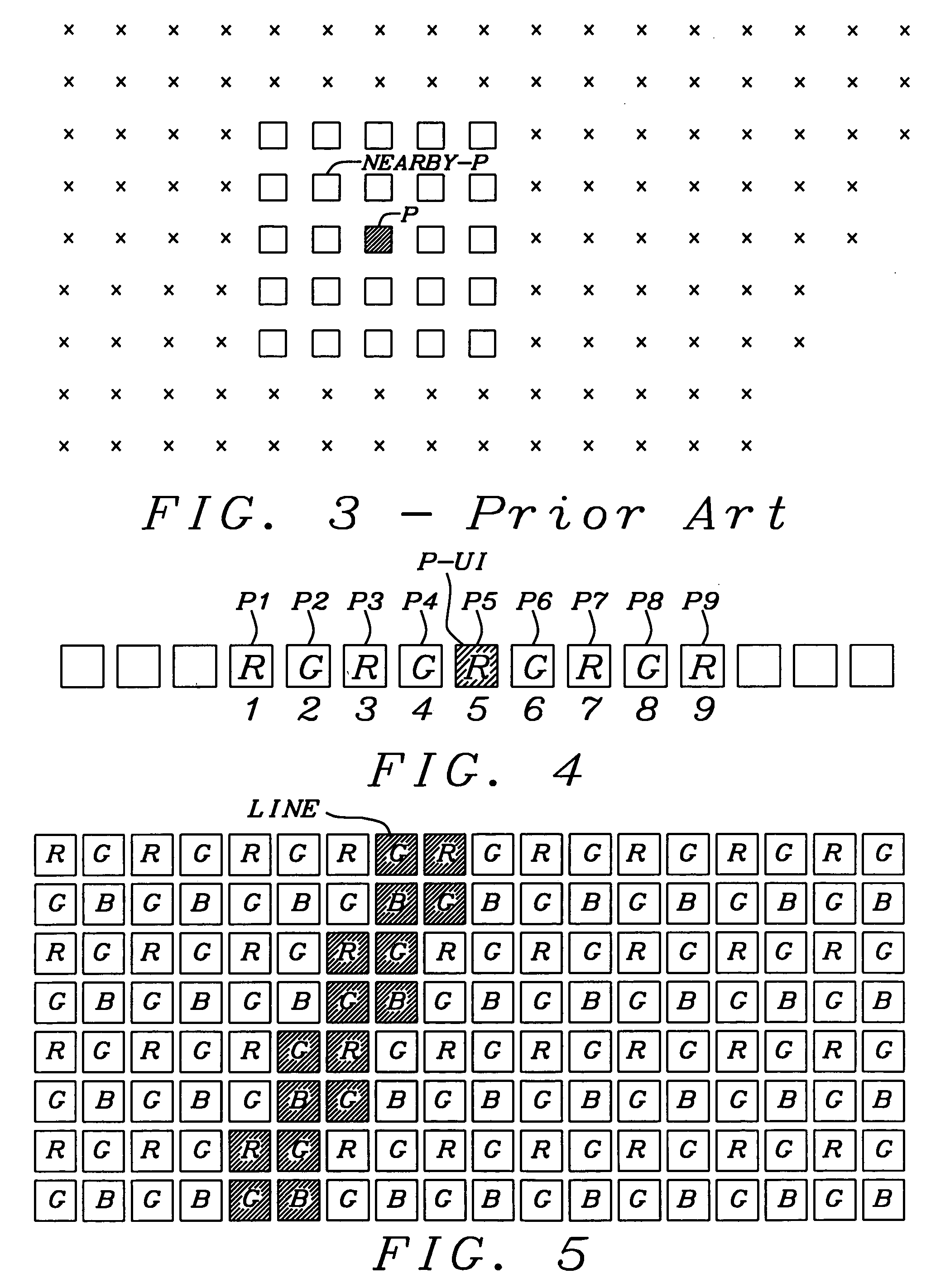
[0023] In large arrays of image sensing devices, arranged in a matrix of rows and columns, like CCDs, a small number of defective image elements (pixels), caused by a variety of manufacturing deficiencies, must be tolerated, especially for low cost applications. The reason may be, for example, manufacturing process defects, which may show up as dead spots (totally dark), hot spots (totally white) and weak spots. Such a defective pixel is generated not only as an initial defect, but it is also generated because of aging, as the solid-state image pick-up device is used for a long period time. Similar, such defective pixels may change with operating conditions, like temperature of the sensor or its supply voltage. The position of the defective pixel itself is fixed. Therefore, the image signal from the defective pixel is often corrected by storing the position thereof in ...


PUM


Abstract

In large arrays of image sensing devices, like CCDs, a small number of defective image elements (pixels) must be tolerated and the resulting image degradation should be eliminated through bad pixel correction. The disclosed invention provides a mechanism to effectively detect defective pixels “on the fly” in a Bayer RGB type color image sensor, optimized for low cost applications. It calculates a variable threshold based on signal changes on nearby pixels of the same color within a single row and checks if the signal change of the pixel under test exceeds said variable threshold. It further performs a plausibility check using nearby pixels of an other color in the same row.

Description

BACKGROUND OF THE INVENTION [0001] (1) Field of the Invention [0002] The present invention relates to a defective pixel correction circuit for correcting a defective pixel in a solid imaging device and, more particularly, to charge coupled device (CCD) and CMOS imagers as used in digital cameras, employing a pixel correction circuit with reduced memory requirements. [0003] (2) Description of Prior Art [0004] In large arrays of image sensing devices, arranged in a matrix of rows and columns, like CCDs a small number of defective image elements (pixels), caused by a variety of manufacturing deficiencies, must be tolerated, especially for low cost applications. The reason may be, for example, manufacturing process defects, which may show up as dead spots (totally dark), hot spots (totally white) and weak spots. Such a defective pixel is generated not only as an initial defects, but it is also generated because of aging, as the solid-state image pick-up device is used for a long period ...

Claims


Application Information

Patent Timeline
IPC IPC(8): G06K9/40H04N1/46H04N3/14H04N5/367H04N9/04H04N9/083H04N9/64
CPCH04N9/045H04N5/3675H04N25/683H04N23/843H04N25/134
Inventor SCHWENG, DETLEF
Owner DIALOG IMAGING SYST
Why Eureka
Try Eureka