
Techniques for spin-flop switching with offset field
a technology of offset field and spin-flop, which is applied in the direction of spin-exchange-coupled multilayers, magnetic bodies, substrate/intermediate layers, etc., can solve the problem of low operating power, soft error rate due to thermally activated switching, and unintentional orientation change of magnetization of one or more magnetic memory cells. to achieve the effect of reducing the switching field
- Summary
- Abstract
- Description
- Claims
- Application Information
AI Technical Summary
Benefits of technology
Problems solved by technology
Method used
Image

Examples
Embodiment Construction
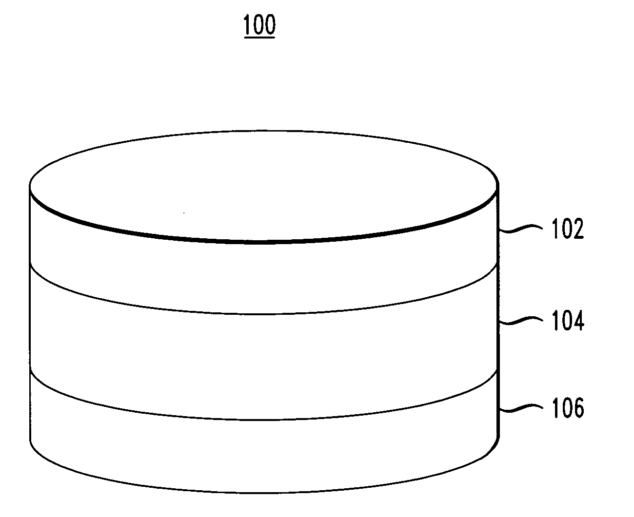
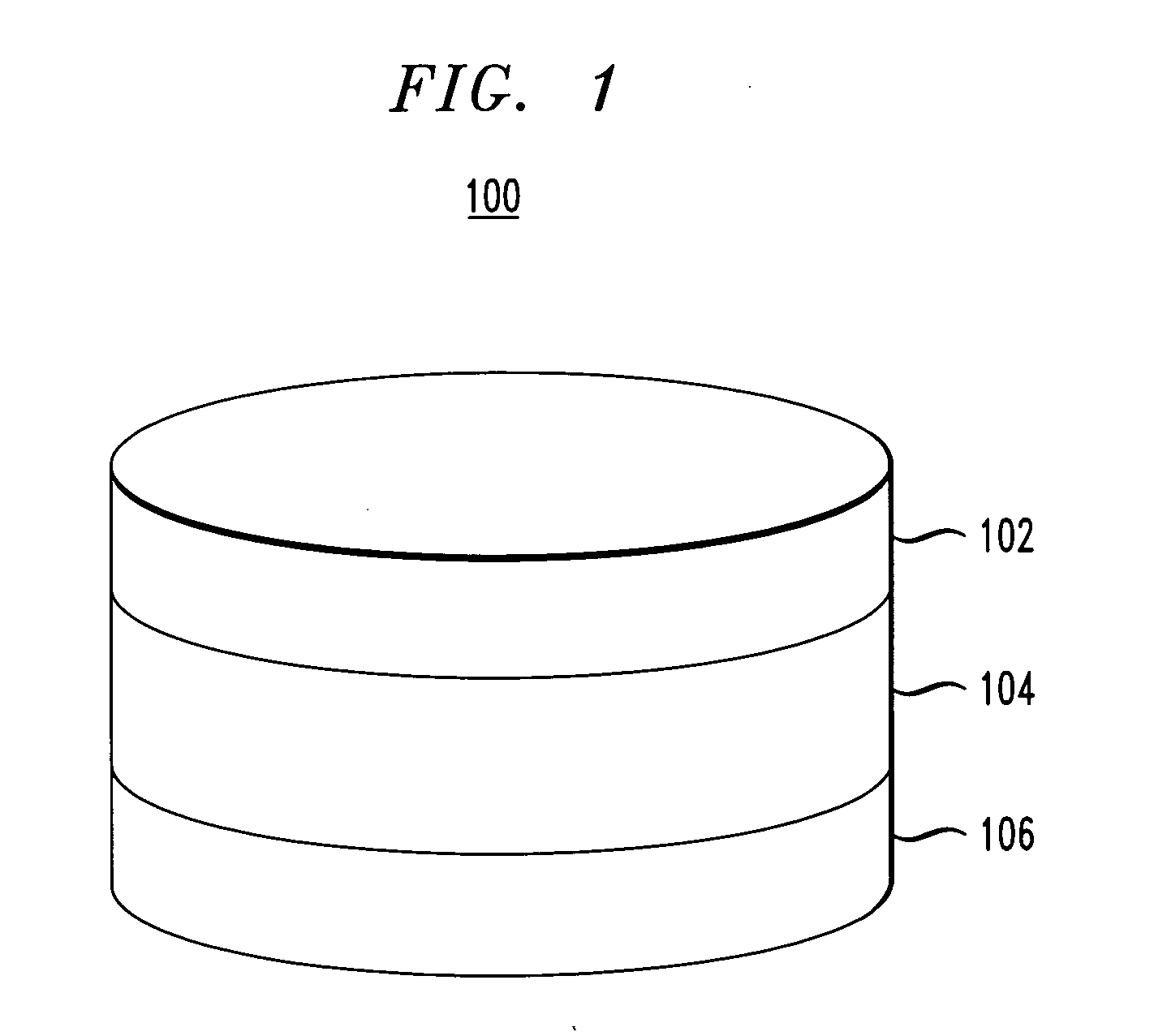
[0021]FIG. 1 is a diagram illustrating an exemplary semiconductor device 100. Semiconductor device 100, which may comprise a magnetic storage element in a magnetic random access memory (MRAM), comprises a first magnetic layer 102, spacer layer 104 and a second magnetic layer 106. Magnetic layers 102 and 106, as shown in FIG. 1, have a substantially elliptical shape. However, in accordance with the teachings presented herein, each of magnetic layers 102 and 106 may have any suitable non-elliptical shape, such as a substantially circular shape.
[0022] Each of magnetic layers 102 and 106 may comprise an element including, but not limited to, nickel, cobalt, iron, manganese and combinations comprising at least one of the foregoing elements. In an exemplary embodiment, first magnetic layer 102 and / or second magnetic layer 106 comprises Ni80Fe20. The composition of magnetic layer 102 may be the same as the composition of magnetic layer 106. Alternatively, the composition of magnetic layer...
PUM
| Property | Measurement | Unit |
|---|---|---|
| thickness | aaaaa | aaaaa |
| thickness | aaaaa | aaaaa |
| thickness | aaaaa | aaaaa |
Abstract
Description
Claims
Application Information