Method for integrating pre-fabricated chip structures into functional electronic systems

Active Publication Date: 2005-11-17
CALIFORNIA INST OF TECH
View PDF6 Cites 19 Cited by
  • Summary
  • Abstract
  • Description
  • Claims
  • Application Information

AI Technical Summary

Benefits of technology

[0020] 6. High-density of electrical connections (e.g., 10,000 per mm2 or larger) is possible.
[0021] In a specific embodiment, an impediment to the fabrication of complex electronics (including but not limited to electrical and mechanical sensors) is the difficulty inherent in fabrication from scratch of an entire device that include chips such as integrated circuits (ICs). This is because IC fabrication often requires very high precision, and usually uses processes that are not easily compatible with sensor fabrication modalities. As such, these ICs are usually fabricated on a wafer at foundries throughout the country, are diced into chips, and are wire-bonded or sometimes

Problems solved by technology

An integrated circuit or chip fabrication facility can cost hundreds of millions, or even billions, of U.S. dollars.
Making devices smaller is very challenging, as each process used in integrated fabrication has a limit.
Additionally, as devices require faster and faster designs, process limitations exist with

Method used


Image

  • Method for integrating pre-fabricated chip structures into functional electronic systems
  • Method for integrating pre-fabricated chip structures into functional electronic systems
  • Method for integrating pre-fabricated chip structures into functional electronic systems

Examples


examples

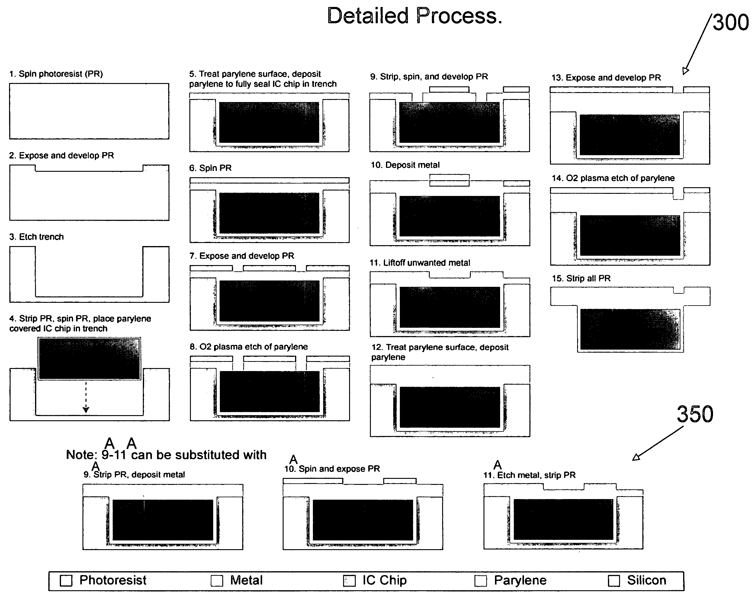
[0151] To prove the principles and operation of the present invention, we have provided examples of the invention in an effort to manufacture bio-compatible integrated circuit chip structures in a flexible substrate design. Such examples are merely illustrative and should not unduly limit the scope of the claims herein. One of ordinary skill in the art would recognize many variations, modifications, and alternatives. Further details of the present experiments are described below according to the figures.

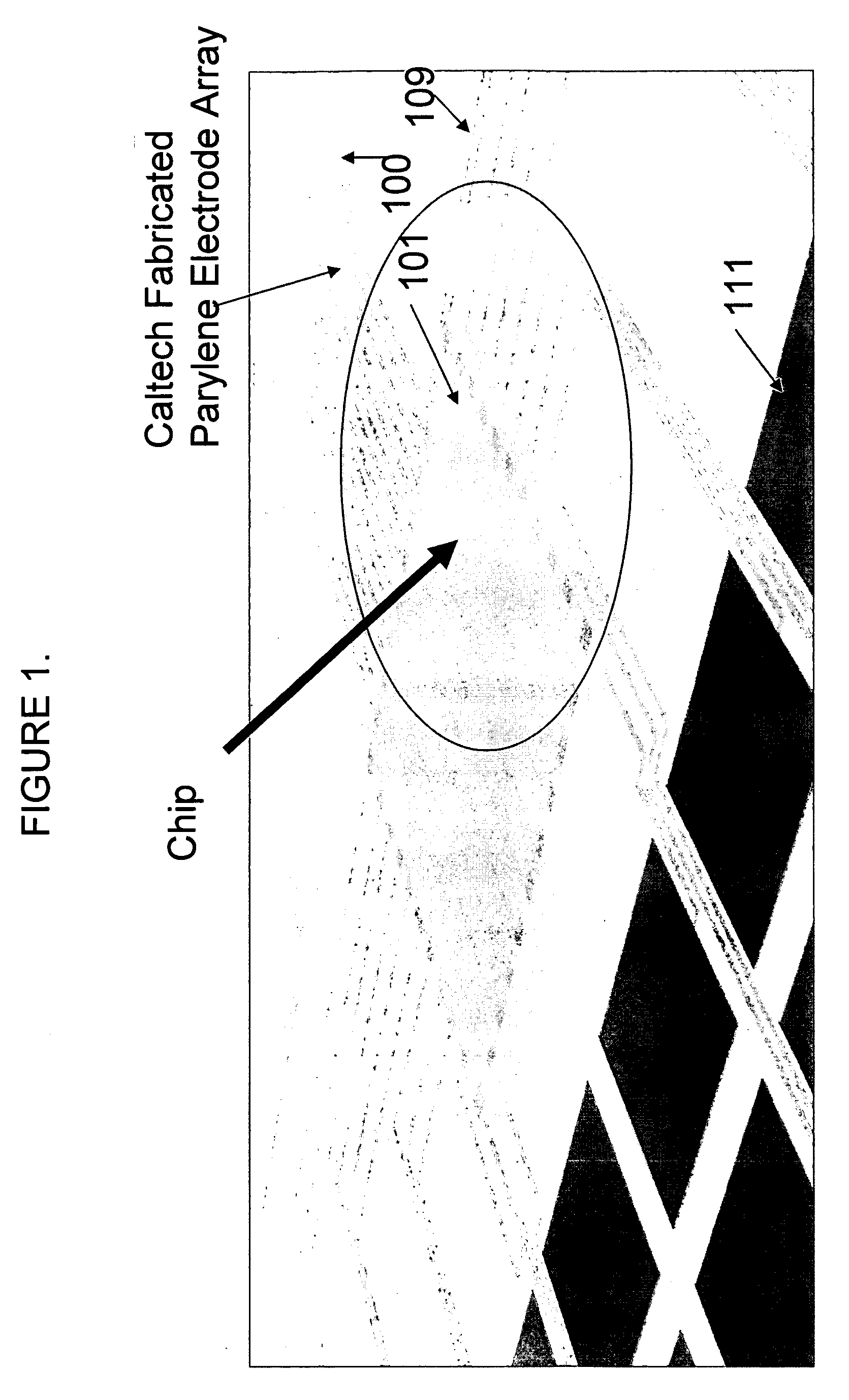
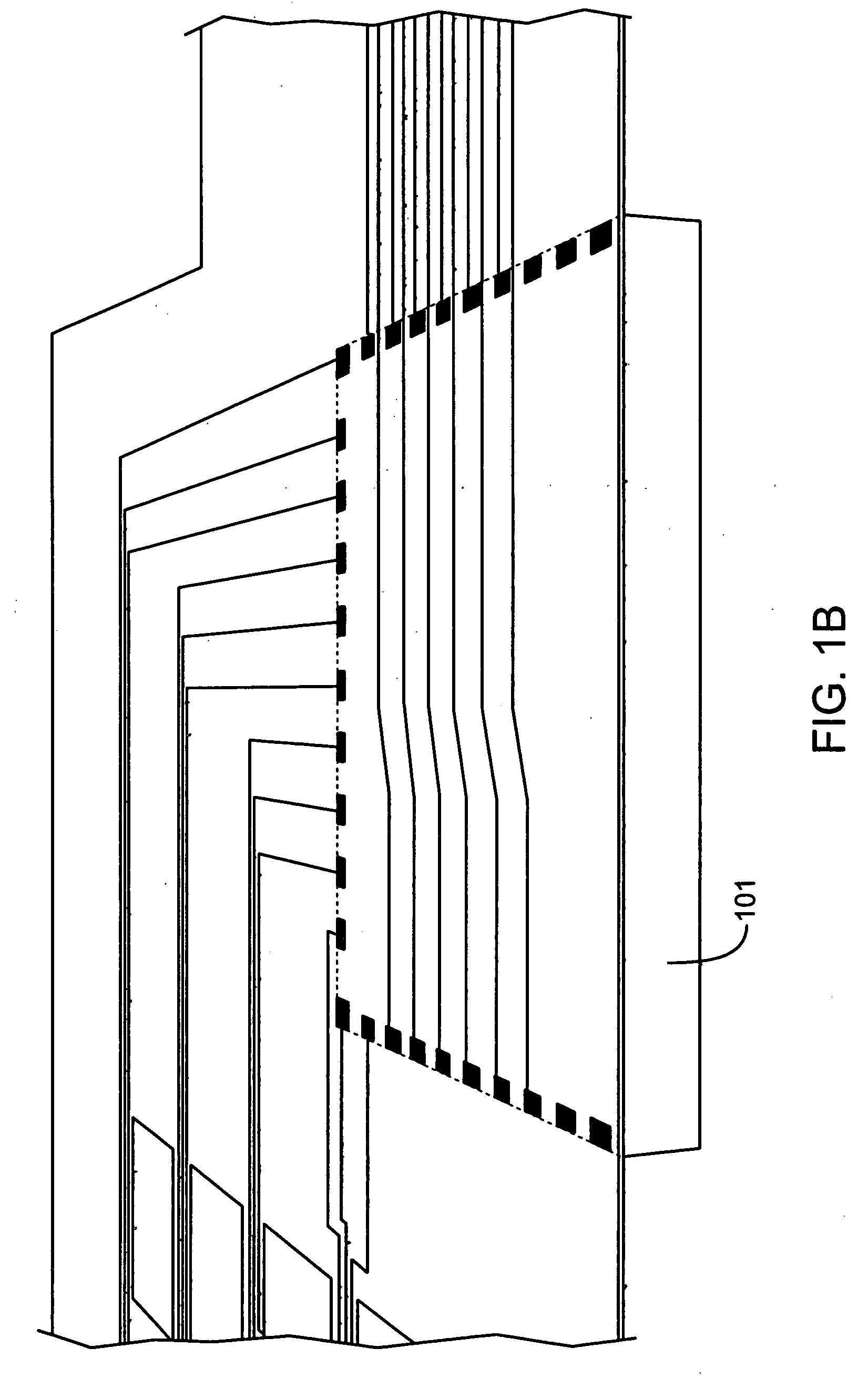
[0152]FIGS. 7-15 are simplified diagrams of experimental results according to embodiments of the present invention. These diagrams are merely examples, which should not unduly limit the scope of the claims herein. One of ordinary skill in the art would recognize many variations, modifications, and alternatives. More particularly, we have focused our experiments on an intraocular retinal prosthesis. As background information, retinal prosthesis includes a wide array of technologies, ...


PUM


Abstract

A method for manufacturing integrated objects, e.g., electronic devices, biological devices. The method includes providing a holder substrate, which has at least one recessed region, the recessed region having a predetermined shape. The holder substrate has a selected thickness and is characterized as being substantially rigid in shape. The method includes aligning a chip comprising a face and a backside into the predetermined shape of the recessed region and disposing the chip into the recessed region. The chip is secured into the recessed region. The method includes providing a first film of insulating material having a first thickness overlying the face and portions of the holder substrate to attach the chip to a portion of the first film of insulating material and patterning the first film of insulating material to form at least one opening through a portion of the first thickness to a contact region on the face of the chip. The method includes forming a metallization layer overlying the first film of insulating material to couple to the contact region through the one opening and forming a protective layer overlying the metallization layer. The method includes releasing the chip from the holder substrate while maintaining attachment of the chip to the first film of insulating material.

Description

CROSS-REFERENCES TO RELATED APPLICATIONS [0001] This application claims priority to U.S. Provisional Patent Application Ser. No. 60 / 517,432 filed Nov. 5, 2003, commonly assigned, and hereby incorporated by reference herein.BACKGROUND OF THE INVENTION [0002] The present invention is directed to manufacturing objects. More particularly, the invention provides a method and resulting structure for integrating a chip structure onto a film of flexible material. Merely by way of example, the invention has been applied to integrated circuit chips provided on polymer based structures such as a film of parylene material. But it would be recognized that the invention has a much broader range of applicability. For example, the invention can be applied to other chip structures including discrete electronic components, micro-electrical mechanical systems (MEMS), nano-electrical mechanical systems (NEMS), displays, power supplies, biological chips, medical chips, and biomedical chips. Additionally...

Claims


Application Information

Patent Timeline
IPC IPC(8): H01LH01L21/44H01L21/60H01L21/68H01L23/538H01L29/40
CPCB81C1/0023B81C1/00333H01L2924/1461H01L2224/24137H01L2924/12041H01L21/561H01L21/568H01L21/6835H01L23/5387H01L23/5389H01L24/19H01L24/97H01L2221/68345H01L2224/04105H01L2224/20H01L2224/211H01L2224/97H01L2924/01013H01L2924/01015H01L2924/01029H01L2924/01047H01L2924/01057H01L2924/01061H01L2924/01074H01L2924/01077H01L2924/01078H01L2924/01079H01L2924/01082H01L2924/12044H01L2924/14H01L2924/1433H01L2924/19043H01L2924/01006H01L2924/01023H01L2924/01033H01L2924/1815H01L2224/82H01L2924/00H01L2924/12042H01L2224/96H01L23/3171H01L23/3185
Inventor TAI, YU-CHONGRODGER, DAMIEN C.
Owner CALIFORNIA INST OF TECH
Why Eureka
Try Eureka