Delay calculation method, timing analysis method, calculation object network approximation method, and delay control method

a timing analysis and calculation method technology, applied in the field of timing analysis methods, can solve the problems of inability to consider cross-talk delay calculation, and inability to perform verification, so as to achieve the effect of controlling the delay time of the driven n

Inactive Publication Date: 2005-11-17
PANASONIC CORP
View PDF16 Cites 6 Cited by
  • Summary
  • Abstract
  • Description
  • Claims
  • Application Information

AI Technical Summary

Benefits of technology

[0044] This structure is a delay value control method in which, for example, when there is a driven net whose wire delay time is necessarily controlled in a semiconductor integrated circuit, the transistor that drives the adjacent wire is changed to a plurality of or a plurality of pairs of transistors, switching is made between a transistor having a driving force required when the adjacent wire makes a state transition and a transistor used for fixing the potential in the steady state, the resistance value connected to the adjacent wire and the power source / ground is changed, and the delay value of the driven net is controlled. By switching the driving transistor of the signal wire driven by a plurality of pairs of transistors, the resistance value between the signal wire and the power source / ground is changed and the effective inter-wire capacitance between the driven net and the adjacent wire is controlled, whereby the delay time of the driven net can be controlled.
[0045] According to this technique, even in LSIs in which the space for the adjacent wire track of the driven net is tight, by changing the driving transistor of the adjacent wire to a plurality of transistors without the provision of a shielding wire and switching between the transistors, the influence of the adjacent wire on the delay time is suppressed, whereby the delay time of the driven net can be controlled.

Problems solved by technology

Therefore, when a corner case timing verification is to be performed, such a verification cannot be performed or it is necessary to leave large equal margins.
Moreover, when an approximation to equally ground inter-wire capacitances is performed, a delay calculation considering cross talk cannot be performed.

Method used


Image

  • Delay calculation method, timing analysis method, calculation object network approximation method, and delay control method
  • Delay calculation method, timing analysis method, calculation object network approximation method, and delay control method
  • Delay calculation method, timing analysis method, calculation object network approximation method, and delay control method

Examples


first embodiment

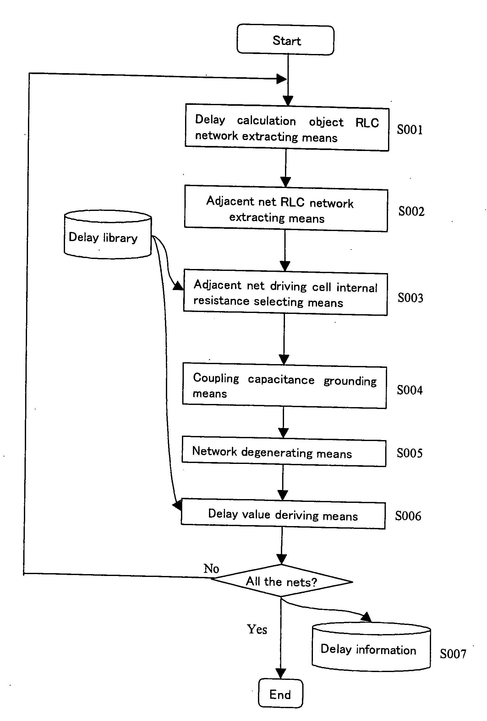
[0078] First, a delay calculation method in designing a semiconductor integrated circuit according to a first embodiment of the present invention will be described with reference to FIGS. 1 to 6. The first embodiment is a delay calculation method considering the influence of nets adjacent to the delay calculation object net in the delay calculation, on the delay value of the delay calculation object net.

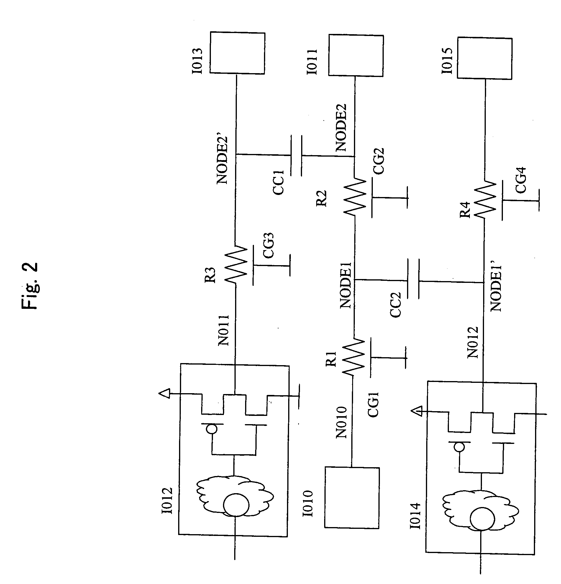
[0079]FIG. 1 is a flowchart showing the procedure of the delay calculation method according to the first embodiment. FIG. 2 is a diagram of a circuit comprising: a net N010 comprising an instance I010 and an instance I011; a net N011 comprising an instance I012 and an instance I013; and a net N012 comprising an instance I014 and an instance I015. The net N010 is coupled to the net N011 through an inter-wire capacitance CC1, and coupled to the net N012 through an inter-wire capacitance CC2. Wire resistances R1 and R2 and ground capacitances CG1 and CG2 are parasitic on the net N010, ...

second embodiment

[0083] A delay calculation method in designing a semiconductor integrated circuit according to a second embodiment of the present invention will be described with reference to FIGS. 2 to 4 and 7 to 9. The second embodiment is a delay calculation method considering the influence of nets adjacent to the delay calculation object net in the delay calculation, on the delay value of the delay calculation object net.

[0084]FIG. 7 is a flowchart showing the procedure of the delay calculation method according to the second embodiment. FIG. 2 is a diagram of a circuit comprising: a net N010 comprising an instance I010 and an instance I011; a net N011 comprising an instance I012 and an instance I013; and a net N012 comprising an instance I014 and an instance I015. The net N010 is coupled to the net N011 through an inter-wire capacitance CC1, and coupled to the net N012 through an inter-wire capacitance CC2. Wire resistances R1 and R2 and ground capacitances CG1 and CG2 are parasitic on the net...

third embodiment

[0088] A timing analysis method, in particular a static timing analysis method in designing a semiconductor integrated circuit according to a third embodiment of the present invention will be described.

[0089] The third embodiment is a timing analysis method where an analysis that is stricter in terms of timing is performed on a setup / hold timing restriction in consideration of the influence of a net adjacent to a net in a timing analysis object path, on the delay value of the net in the timing analysis object path.

[0090]FIG. 10 is a flowchart showing the procedure of the timing analysis method according to the third embodiment. FIG. 11 shows a synchronous sequential circuit having: a net N020 from a clock source CK to a flip-flop FF1; a net N023 from the clock source CK to a flip-flop FF2; a combinational circuit COMB1 and a net N021 which are a path from the flip-flop FF1 to the flip-flop FF2; a net N024 adjacent to the net N020; a net N025 adjacent to the net N021; and a net N02...


PUM


Abstract

A delay calculation method considering a net adjacent to a delay calculation object net of a semiconductor integrated circuit includes: an adjacent net internal resistance selecting step of selecting a combination of static state of an adjacent net driving cell; a coupling capacitance grounding step of multiplying a coupling capacitance by a coefficient obtained from an internal resistance of the adjacent net driving cell selected by the adjacent net internal resistance selecting step, and the like, and grounding the value obtained thereby as the coupling capacitance of the delay calculating object net; and a delay value deriving step of deriving the delay value from a circuit obtained by these steps. A problem of the delay calculation method that an accurate delay value cannot be obtained because in actuality, the adjacent wire whose potential fluctuates is approximated to zero potential is solved by this structure.

Description

BACKGROUND OF THE INVENTION [0001] 1. Field of the Invention [0002] The present invention relates to a delay calculation method, a timing analysis method, a calculation object network approximation method and a delay control method that are used for CAD apparatuses and the like for aiding the designing of semiconductor devices and speed up the delay time as a whole or speed up a given wire in the produced semiconductor device. [0003] 2. Description of the Prior Art [0004] In recent years, since the semiconductor process has become finer and the capacitance stored between adjacent wires has been increased with respect to the substrate capacitance and the gate capacitance, performing a delay calculation considering the inter-wire capacitance by use of a CAD apparatus has been mainstream. Further, a method is commonly performed in which the potential fluctuation time of an adjacent wire is analyzed with a time width by a static analysis method and the delay fluctuation due to the inter...

Claims


Application Information

Patent Timeline
Patent Type & Authority Applications(United States)
IPC IPC(8): G06F17/50G06G7/00H01L21/82H01L27/04H03K5/14
CPCG06F17/5036G06F30/367
Inventor AMEKAWA, NAOKIICHINOMIYA, TAKAHIROSATOH, KAZUHIRO
Owner PANASONIC CORP
Why Eureka
Try Eureka