Simple CMOS light-to-current sensor

Inactive Publication Date: 2005-11-24
CHEN PAO JUNG
View PDF13 Cites 9 Cited by
  • Summary
  • Abstract
  • Description
  • Claims
  • Application Information

AI Technical Summary

Benefits of technology

[0009] This invention demonstrates a very small, high performance, and cost-effective CMOS light-to-current sensor whi

Problems solved by technology

The trans-impedance amplifier of the light-to-voltage sensor is quite complicated to implement as an integrated circuit, and the current amplifier of th

Method used


Image

  • Simple CMOS light-to-current sensor
  • Simple CMOS light-to-current sensor
  • Simple CMOS light-to-current sensor

Examples


Embodiment Construction

[0018] The photo-detector of this invention is a CMOS light-to-current sensor which is comprised of a photo-diode and two MOS transistors.

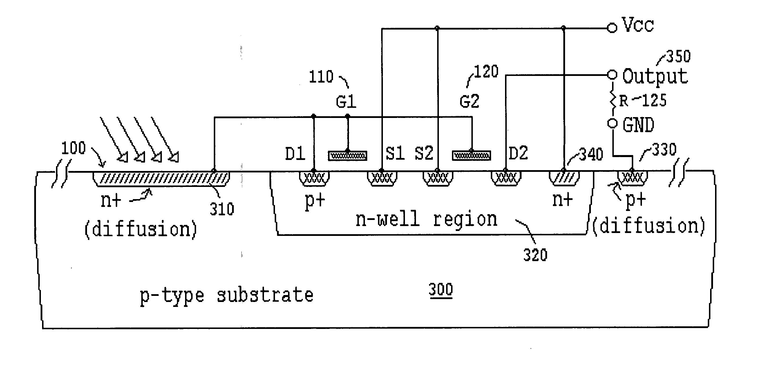
[0019] Referring to FIG. 3 of the present invention, a CMOS light-to-current sensor built on a p-type substrate wafer is illustrated, the photo-diode is an n+-p junction photo-diode and the two MOS transistors are p-channel transistors built in the n-well region. Also referring to FIG. 4 of the present invention, a CMOS light-to-current sensor built on an n-type substrate wafer is illustrated, the photo-diode is a p+-n junction photo-diode and the two MOS transistors are n-channel transistors built in the p-well region.

[0020] As illustrated in FIG. 5, in a typical CMOS n-well process technology using a p-type substrate wafer, the photo-diode is constructed by an n+ diffusion layer thermally-diffused on top of the p-type substrate, and the two MOS transistors are p-channel transistors built in the n-well region. As illustrated in FIG. 3, the circ...


PUM


Abstract

A CMOS light-to-current sensor built on silicon substrate is disclosed in this invention. This light-to-current sensor includes a photo-diode and two MOS transistors. The first MOS transistor is connected as the load transistor for the photo-generated current from the photo-diode, and the second MOS transistor is connected as the current-mirror transistor for the first transistor to output a current linearly proportional to the photo-generated current to the external resistor connected to the sensor.

Description

TECHNICAL FIELD OF THE INETION [0001] This invention relates to a photo-detector used as a photometer to provide a measurement of the amount of light power incident on the detector. Particular applications for these photometers include power-saving control for street lights and domestic appliances, back-lighting of displays in cellular phones, notebook PCs, PDAs, video cameras, digital still cameras, and other equipment requiring luminosity adjustment. BACKGROUND OF THE INVENTION [0002] A photometer IC can be constructed by using a light-to-voltage sensor or a light-to-current sensor. A light-to-voltage sensor combines a photo-diode and a trans-impedance amplifier on a single monolithic IC, such as the TSL251R light-to-voltage optical sensor (1) described in its data sheet by Texas Advanced Optoelectronic Solutions Inc., and is illustrated in FIG. 1. The trans-impedance amplifier senses the current generated by the photo-diode and outputs a voltage proportional linearly to the photo...

Claims


Application Information

Patent Timeline
IPC IPC(8): G01J1/44H01L27/146H01L31/00H01L31/08
CPCG01J1/44H04N5/35518H01L27/14609H04N25/573
Inventor CHEN, PAO JUNG
Owner CHEN PAO JUNG
Why Eureka
Try Eureka