Semiconductor memory device having a global data bus

a global data bus and memory device technology, applied in the direction of information storage, static storage, digital storage, etc., can solve the problems of increasing the problem of coupling noise between adjacent global data bus lines, issuance of data errors under serious state, and small layout area for routing the global data bus, so as to achieve the effect of reducing coupling nois

Active Publication Date: 2005-11-24
SK HYNIX INC
View PDF12 Cites 8 Cited by
  • Summary
  • Abstract
  • Description
  • Claims
  • Application Information

AI Technical Summary

Benefits of technology

[0015] It is, therefore, a primary object of the present invention to provide to a semiconductor memory device that is capable of alleviating coupling noise, without an expansion of line interval of a global data bus.

Problems solved by technology

Thus, signals on adjacent global data bus lines may be affected by noises due to coupling, resulting in an issuance of data errors under the serious state.
However, as the memory chip becomes high integrated, the enlargement of the bank region is inevitable and thus the layout area for routing of the global data bus becomes relatively small.
Meanwhile, since it is expected that the future memory chip supports more wide bandwidth and is provided with the global data bus of 32 or 64 bits, it will be apparent that the coupling noise between the adjacent global data bus lines would occur more serious problem.
As another scheme, meanwhile, there may be an idea that makes the layout sequence of the global data bus lines random, contrary to the concept that arraying the global data lines sequentially results in maximum coupling noise.
In this case, the total coupling noise amount of the global data bus may decrease compared to the existing method shown in FIG. 1, but makes a length of the overlap interval for each line inconstant.
This may result in a problem allowing a different delay time for each line.
In this case, there may be a need of an extra circuit for removing skew between the global data bus lines, and also may be a difficulty to guarantee the chip's operation characteristics since the skew by lines is also random although the skew circuit is utilized while yielding damage to the chip area.

Method used


Image

  • Semiconductor memory device having a global data bus
  • Semiconductor memory device having a global data bus
  • Semiconductor memory device having a global data bus

Examples


first embodiment

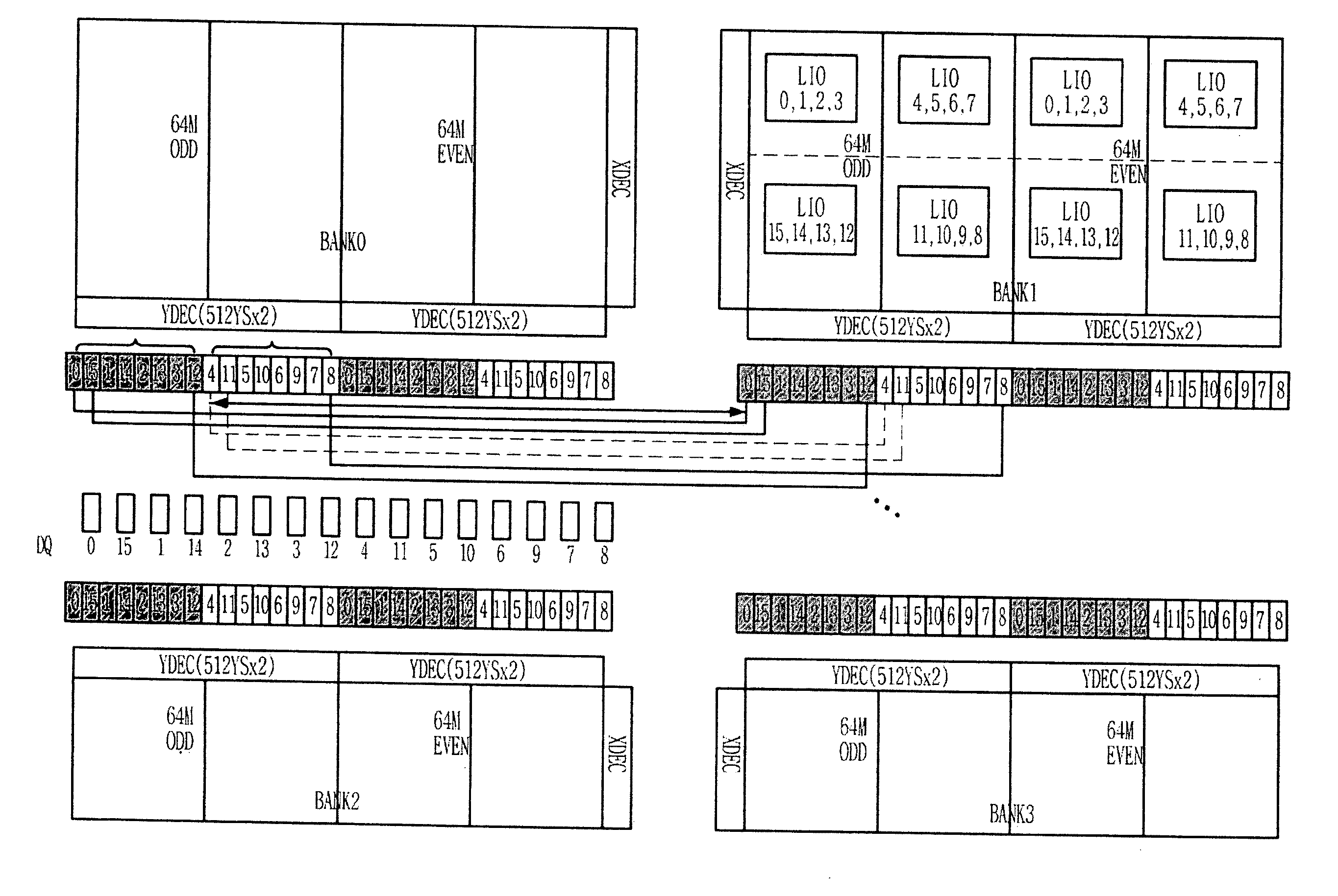
[0023] In accordance with the present invention, there is provided a semiconductor memory device having a plurality of banks comprising: a plurality of input / output (I / O) pads prepared for data input and output; a global data bus arranged between banks neighboring in a first direction and the I / O pads; and a plurality of data transmission units for data transmission between each bank and the global data bus, wherein the data transmission units corresponding to said each bank are classified into a multiplicity of groups, each group having plural continuous data transmission units, and bus lines in the first direction of the global data bus corresponding to each data transmission unit are arranged sequentially and alternately for each group.

[0024] Herein, it is desirable that bus lines in the first direction of the global data bus corresponding to the data transmission units included in each group are arranged in sequence.

[0025] Further, it is preferable that the arrangement order of...

second embodiment

[0026] In accordance with the present invention, there is provided a semiconductor memory device comprising: a plurality of banks having a first and a second cell regions, which share one row decoder and are unit region selected by a first and a second column decoders; a plurality of input / output (I / O) pads prepared for data input and output; a global data bus arranged between banks neighboring in a first direction and the I / O pads; a plurality of first data transmission units for data transmission between the first cell region and the global data bus; and a plurality of second data transmission units for data transmission between the second cell region and the global data bus, wherein bus lines in the first direction of the global data bus corresponding to the first and the second data transmission units are arranged sequentially and alternately for each cell region.

[0027] Herein, it is desirable that bus lines in the first direction of the global data bus corresponding to one data...

third embodiment

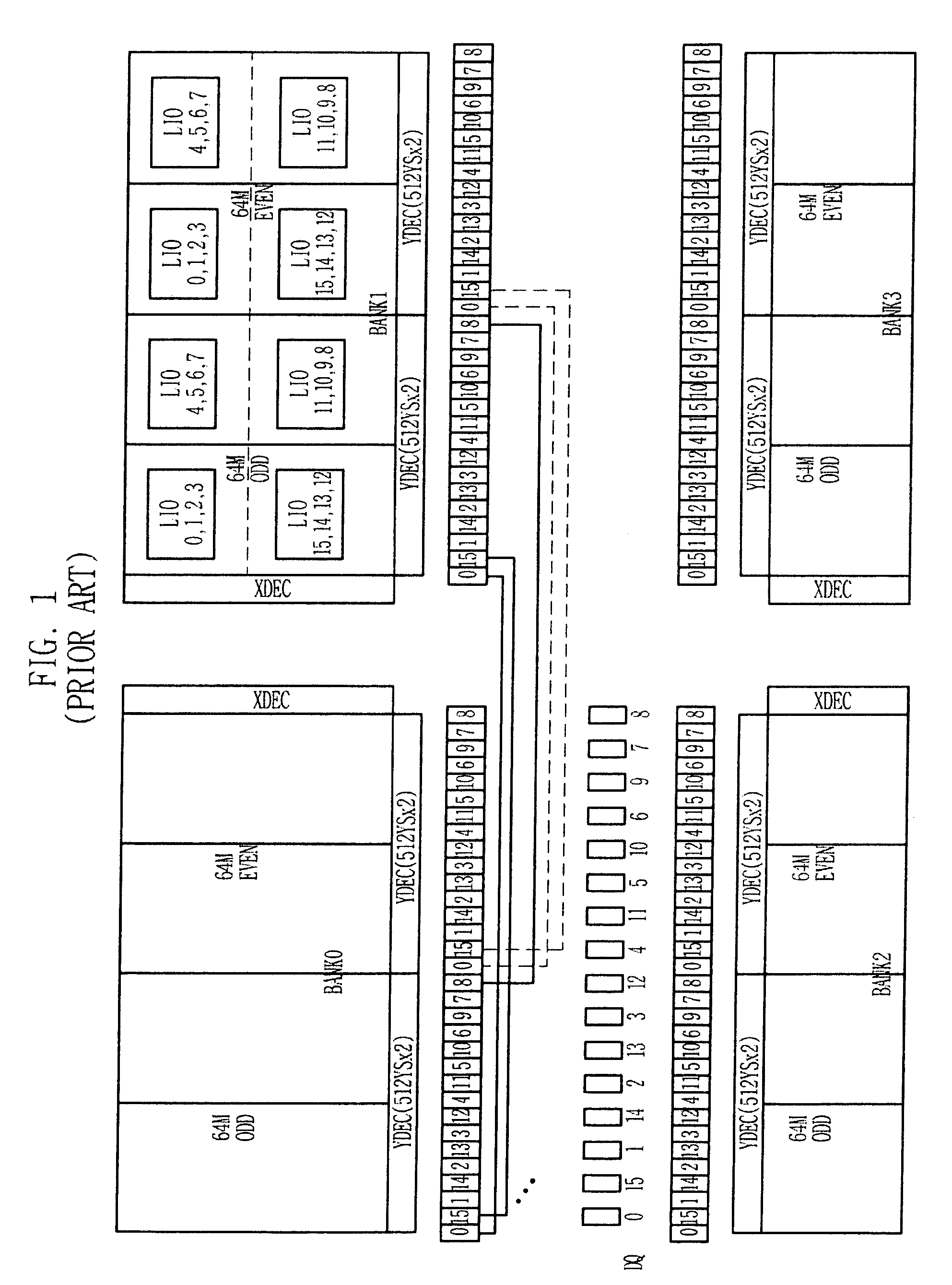
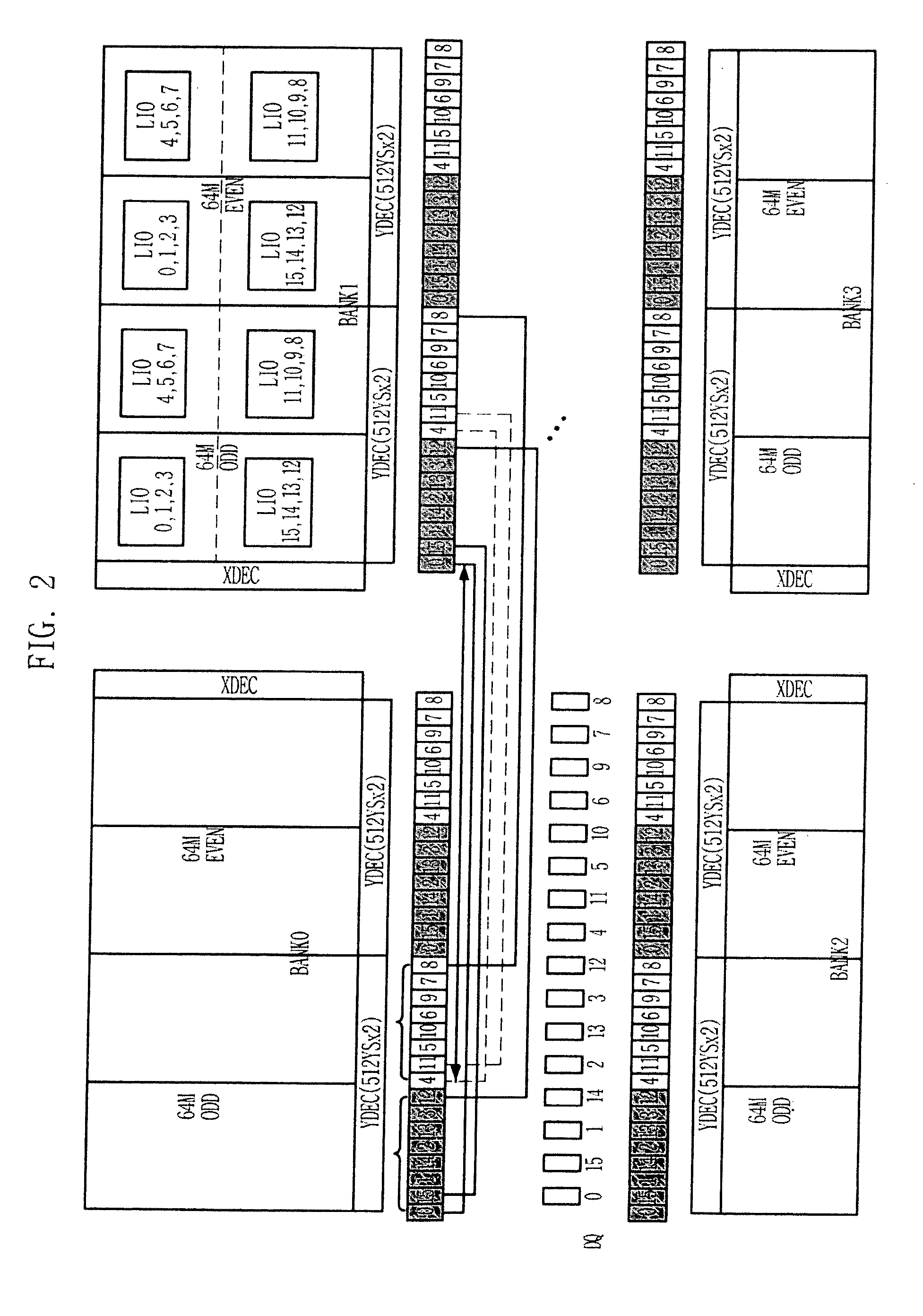
[0029] In accordance with the present invention, there is provided a semiconductor memory device having a plurality of banks comprising: 16 input / output (I / O) pads for data input and output, which are arranged in the order of 0, 15, 1, 14, 2, 13, 3, 12, 4, 11, 5, 10, 6, 9, 7, and 8; a global data bus arranged between a first and a second banks neighboring in a row direction and the 16 I / O pads; and 16 data transmission units for data transmission between each bank and the global data bus, which are arranged in the order of 0, 15, 1, 14, 2, 13, 3, 12, 4, 11, 5, 10, 6, 9, 7, and 8.


PUM


Abstract

There is provided a semiconductor design technology, particularly, a bus line arrangement method of global data bus in the semiconductor memory device. According to the invention, skew by lines can be not occurred, or can be minimized upon an issuance thereof. Further, upon its issuance, it is easy to compensate it relying on the specific rule. The present invention proposes a scheme that classifies data transmission units corresponding to each bank into plural groups, each group having some continuous data transmission units, and makes bus lines of the global data bus to be arranged alternately for each group. In other words, the global data bus line arrangement scheme suggested by the present invention may be defined as grouped alternate arrangement scheme. In this case, the overlap interval between adjacent global data bus lines can be reduced largely and skew problem by lines can also be solved.

Description

FIELD OF THE INVENTION [0001] The present invention relates to a semiconductor design technology; and, more particularly, to a bus line arrangement of a global data bus GIO in a semiconductor memory device. BACKGROUND OF THE INVENTION [0002] As is well known, most of semiconductor memory devices including DRAM have a hierarchical I / O bus structure. In other words, those devices have a structure that connects global data bus GIO plural banks share to local data bus LIO prepared in each bank hierarchically. [0003] Specifically, the global data bus is coupled with an I / O pad and the local data bus of each bank. In this structure, data transmission unit is needed for data transmission between the global data bus and the local data bus. In general, such data transmission unit comprises a write driver for driving input data on the global data bus onto the local data bus, and an I / O sense amp for loading output data on the local data bus onto the global data bus. [0004] Meanwhile, as a siz...

Claims


Application Information

Patent Timeline
Patent Type & Authority Applications(United States)
IPC IPC(8): G11C5/06G11C8/00G11C11/401G11C11/4093
CPCG11C5/063G11C11/4093G11C8/10G11C5/06
Inventor KIM, KYOUNG-NAMYOON, SEOK-CHEOL
Owner SK HYNIX INC
Why Eureka
Try Eureka