Semiconductor device, manufacturing method therefor, and electronic device

A manufacturing method and semiconductor technology, applied in semiconductor devices, electric solid state devices, circuits, etc., can solve the problem that it is difficult to form air gaps between bit lines, etc., to reduce bit line capacitance, reduce coupling noise, and improve RC delay Effect

Active Publication Date: 2017-12-29
SEMICON MFG INT (SHANGHAI) CORP +1
View PDF8 Cites 3 Cited by
  • Summary
  • Abstract
  • Description
  • Claims
  • Application Information

AI Technical Summary

Problems solved by technology

[0003] In the bit line formation process of the current NAND flash memory, the W or Cu damascene process is often used. First, the oxide film between the bit lines is deposited, then the oxide film is etched, and then deposited to form W or Cu. Therefore, in the bit line It is difficult to form an air gap between

Method used


Image

  • Semiconductor device, manufacturing method therefor, and electronic device
  • Semiconductor device, manufacturing method therefor, and electronic device
  • Semiconductor device, manufacturing method therefor, and electronic device

Examples


Embodiment 1

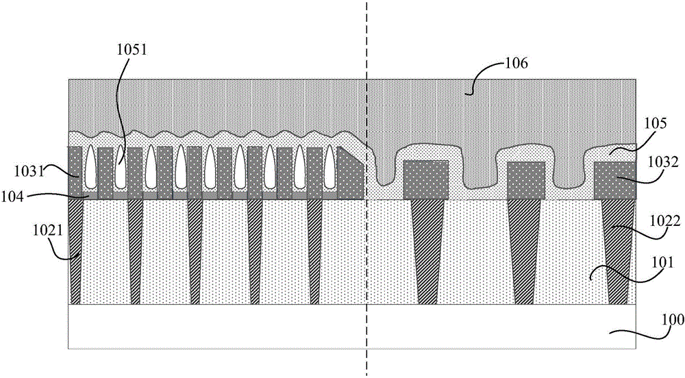
[0056] Refer below figure 1 The semiconductor device of the present invention is described in detail, wherein, figure 1 A cross-sectional view of a semiconductor device in a specific embodiment of the present invention is shown.

[0057] The semiconductor device of the present invention may be any semiconductor device known to those skilled in the art. As an example, the semiconductor device is a NAND flash memory.

[0058] The semiconductor device of the present invention includes the following main structures: a base, the base includes a core area, and an interlayer dielectric layer is arranged on the base; A plurality of first bit lines, wherein the first bit lines extend along a first direction; a first dielectric layer is arranged to cover the first bit lines and the interlayer dielectric layer in the core region, wherein, An air gap is formed in the first dielectric layer between adjacent first bit lines in the core region.

[0059] Specifically, as figure 1 As shown...

Embodiment 2

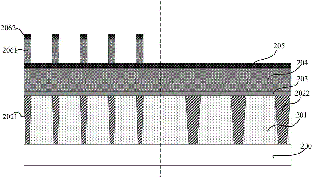
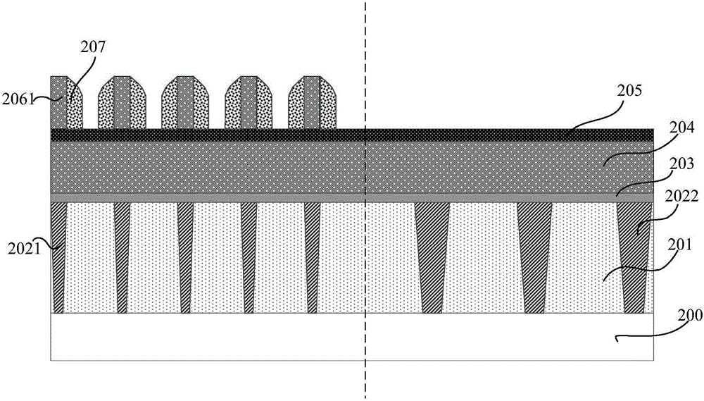
[0094] In view of the superior performance of the above-mentioned semiconductor device, the present invention also provides a manufacturing method of the semiconductor device, such as image 3 As shown, the semiconductor device mainly includes the following steps:

[0095] Step S301: providing a substrate, the substrate includes a core region and a peripheral region, an interlayer dielectric layer is formed on the substrate, and a patterned hard mask layer is formed on the interlayer dielectric layer in the core region , the patterned hard mask layer includes a plurality of openings, the openings corresponding to the predetermined pattern of the first bit line in the core region;

[0096] Step S302: forming a bit line material layer covering the patterned hard mask layer and the exposed interlayer dielectric layer of the core region and the peripheral region;

[0097] Step S303: forming a patterned photoresist layer on the bit line material layer in the peripheral area;

[0...

Embodiment 3

[0165] The present invention also provides an electronic device, including the semiconductor device described in Embodiment 1, and the semiconductor device is prepared according to the method described in Embodiment 2.

[0166] The electronic device of this embodiment can be any electronic device such as a mobile phone, a tablet computer, a notebook computer, a netbook, a game console, a TV set, a VCD, a DVD, a navigator, a digital photo frame, a camera, a video camera, a recording pen, MP3, MP4, PSP, etc. Product or equipment, but also any intermediate product including electrical circuits. The electronic device of the embodiment of the present invention has better performance due to the use of the above circuit.

[0167] in, Figure 4 An example of a mobile phone handset is shown. The mobile phone handset 400 is provided with a display portion 402 included in a housing 401, operation buttons 403, an external connection port 404, a speaker 405, a microphone 406, and the lik...


PUM


Abstract

The invention provides a semiconductor device, a manufacturing method therefor and an electronic device, and relates to the technical field of semiconductors. The semiconductor substrate comprises a substrate which comprises a core region and is provided with an interlayer dielectric layer; a plurality of first bit lines which are disposed on the interlayer dielectric layer in the core region at intervals; a first dielectric layer which covers the first bit lines and the interlayer dielectric layer in the core region, wherein each part, between the adjacent first bit lines in the core region, of the first dielectric layer is provided with an air gap. According to the invention, the air gaps are disposed between the adjacent bit lines of the semiconductor devices, thereby reducing the capacitance of the bit lines, and reducing the coupling noise between the bit lines. Also, units with the uniform performances can be obtained, such as a unit with the uniform threshold voltage (Vt) and a unit with the uniform random telegraph noise. Moreover, the device improves the RC delay of the bit lines, and is enabled to have better performances.

Description

technical field [0001] The present invention relates to the technical field of semiconductors, in particular to a semiconductor device and its manufacturing method and manufacturing method. Background technique [0002] As the size of NAND flash memory shrinks to 2Xnm, 1Xnm nodes and below, the control of the spacing dimension (CD) between adjacent bit lines (Bitline, BL for short) becomes more and more stringent. Therefore, the air gap The (Airgap) scheme has attracted attention because of its following advantages. First, the air gap is used to reduce the capacitance to reduce the coupling noise (coupling noise) between the bit lines. Secondly, by reducing the capacitance, a unit with uniform performance can also be obtained. For example, cells with uniform threshold voltage (Vt), cells with uniform random telegraphic noise (RTN for short), and the use of air gaps can also improve the RC delay of the bit line. [0003] In the bit line formation process of the current NAND ...

Claims


Application Information

Patent Timeline
Patent Type & Authority Applications(China)
IPC IPC(8): H01L27/11517
CPCH10B41/00H10B41/41H10B41/35
Inventor 罗文军杨海玩
Owner SEMICON MFG INT (SHANGHAI) CORP
Why Eureka
Try Eureka