Data input/output (I/O) apparatus for use in memory device

a data input/output and memory device technology, applied in the direction of information storage, static storage, digital storage, etc., can solve the problems of reduced vdd voltage, increased parasitic capacitance, increased coupling noise between lines, etc., and achieve the effect of preventing memory failur

Inactive Publication Date: 2007-01-09
SK HYNIX INC
View PDF4 Cites 4 Cited by
  • Summary
  • Abstract
  • Description
  • Claims
  • Application Information

AI Technical Summary

Benefits of technology

[0020]Therefore, the present invention has been made in view of the above problems, and it is an object of the present invention to provide a data I / O apparatus for use in a memory device, which performs data transmission using the same polarity when neighbor GIO lines have opposite polarities to reduce coupling noise generated between GIO lines acting as data I / O lines of a memory device, performs data recovery, and basically deletes the coupling noise, such that it reduces the failure rate of the memory device.
[0024]Therefore, in the case of GIO lines for transmitting an output signal of the I / O sense amplifier to the output driver capable of outputting the received output signal to a data pad, the above-mentioned data I / O apparatus according to the present invention installs the transceiver for comparing polarities of signals loaded on neighbor GIO lines from among the GIO lines and the receiver for recovering a signal received from the transceiver in the GIO lines, such that it allows data loaded on the neighbor GIO lines to have the same polarity and transmits the data. As a result, the data I / O apparatus basically removes the coupling noise generated by the neighbor GIO lines during transmission of the data, such that it prevents memory failure.

Problems solved by technology

The reduced VDD voltage and the reduced interval between the lines incur increased parasitic capacitance, and coupling noise between the lines is also increased due to the increased parasitic capacitance, such that the increased coupling noise generates a DRAM failure.
A specific phenomenon such as coupling noise frequently occurs in the GIO line.
The above-mentioned method for forming the VSS line in the interval between the GIO lines has a disadvantage in that it frequently incurs noise in the GIO line due to unexpected shaking of the VSS line and thus generally requires an additional repeater.
However, the above-mentioned method for forming the VSS line in the interval between the GIO lines is the most popular method in recent times, and has another disadvantage in that it is unable to basically delete the coupling noise.
The above-mentioned method for employing the test mode line is affected by the GIO line, changes a current polarity to another polarity of a test mode, and affects DRAM operations, resulting in DRAM failure.

Method used


Image

  • Data input/output (I/O) apparatus for use in memory device
  • Data input/output (I/O) apparatus for use in memory device
  • Data input/output (I/O) apparatus for use in memory device

Examples


Embodiment Construction

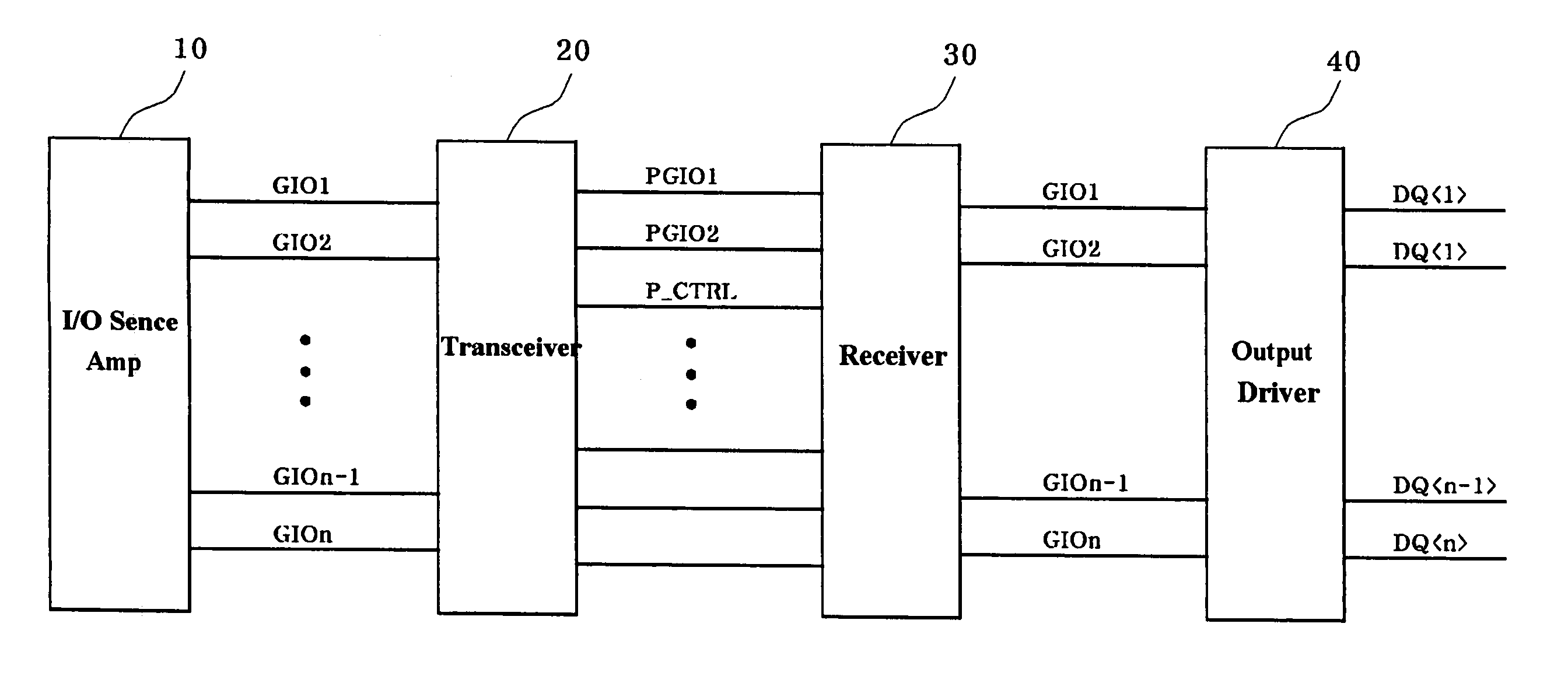
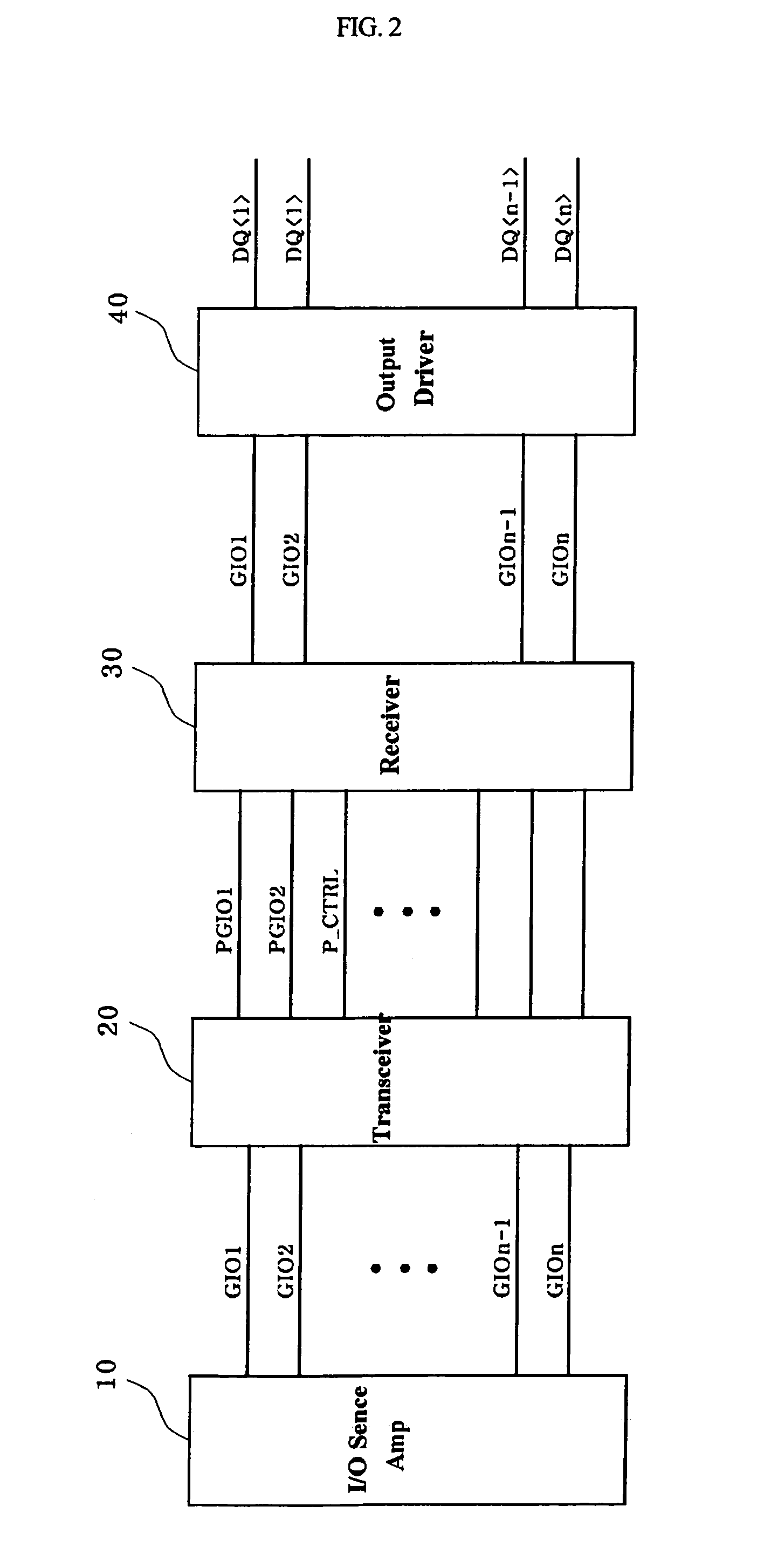
[0030]Now, preferred embodiments of the present invention will be described in detail with reference to the annexed drawings. In the drawings, the same or similar elements are denoted by the same reference numerals even though they are depicted in different drawings. In the following description, a detailed description of known functions and configurations incorporated herein will be omitted when it may make the subject matter of the present invention rather unclear. FIG. 2 is a block diagram illustrating a data I / O apparatus for use in a memory device according to the present invention.

[0031]Referring to FIG. 2, the data I / O apparatus includes an I / O sense amplifier 10 contained in each bank (not shown) of the memory device; a transceiver 20 for receiving a plurality of GIO signals (GIO1˜GIOn) from the I / O sense amplifier 10, comparing the received GIO signals with neighbor GIO signals, converting the GIO signals into other signals having the same polarities as the neighbor GIO sig...


PUM


Abstract

A data I / O apparatus for use in a memory device. The data I / O apparatus for use in the memory device performs data transmission using the same polarity when neighbor global I / O lines have opposite polarities to reduce coupling noise generated between global I / O lines acting as data I / O lines of a memory device, performs data recovery, and basically deletes the coupling noise, such that it reduces the failure rate of the memory device.

Description

[0001]This application relies for priority upon Korean Patent Application No. 2004-25510 filed on Apr. 13, 2004, the content entirety.BACKGROUND OF THE INVENTION[0002]1. Field of the Invention[0003]The present invention relates to a data Input / Output (I / O) apparatus for use in a memory device, and more particularly to a data I / O apparatus for use in a memory device, which performs data transmission using the same polarity when neighbor global I / O lines have opposite polarities to reduce coupling noise generated between global I / O lines acting as data I / O lines of a memory device, performs data recovery, and basically deletes the coupling noise, such that it reduces the failure rate of the memory device.[0004]2. Description of the Related Art[0005]With the increasing development of large-capacity DRAMs and high-speed DRAMs, improved DRAMs, each of which includes a sub wordline drive for operating a word line at a high speed and a hierarchical I / O line structure in which Local Input O...

Claims


Application Information

Patent Timeline
Patent Type & Authority Patents(United States)
IPC IPC(8): G11C7/00G11C11/4096G11C7/02G11C7/10G11C8/00G11C11/4093
CPCG11C5/04G11C7/02G11C11/4093G11C7/1051G11C7/1069G11C7/1048G11C7/06G11C11/4091G11C11/4096
Inventor LEE, SEUNG HUN
Owner SK HYNIX INC
Why Eureka
Try Eureka