Adhesive sheet stamping device, adhesive sheet stamping method, part mounter display panel manufacturing method

Inactive Publication Date: 2005-11-24
PANASONIC CORP
View PDF5 Cites 2 Cited by
  • Summary
  • Abstract
  • Description
  • Claims
  • Application Information

AI Technical Summary

Benefits of technology

[0015] The present invention was conceived to solve the problems described above, and it is an object thereof to provide an adhesive sheet attaching device, a component mounting device, and a display panel production method that use these, which can improve productivity and reduce resource losses.
[0025] Next, a component mounting device of the present invention uses an adhesive sheet attaching device of according to the present invention, and fixes a mounted component to the adhesive sheet that has been attached to the target object by the adhesive sheet attaching device. By using such a component mounting device with the above-mentioned adhesive sheet attaching device, outstanding productivity can be achieved, and resource losses can be reduced.

Problems solved by technology

However, conventional ACF attaching devices such as those described above have the following problems.
When using a reel wound with joined ACF, a portion containing a joint cannot be used for attachment to a substrate.
However, the time when the joint appears varies depending on the length of attachments, and the type of reel, and in most cases it is impossible to ensure that the joint appears at the end of production.
In this case, the ACF containing a joint is peeled off from the release sheet, and in many cases an attachment length longer than a single attachment unit remains in this peeled off portion, so that there are many cases of wastefully peeling off more film than necessary and not making use of and attaching to a substrate the usable limit of ACF up to the joint.
Thus there is the problem of resource loss.
Furthermore, there is also the problem that, after the joint appears, the successive operation of peeling off the joined portion of ACF is a manual task, and therefore takes time in preparation.
Furthermore, when the ACF is provided with an end mark, the usable limit of ACF up to the end mark is not made use of and attached to a substrate when the end mark is recognized.
Thus there is the problem of wasting resources.

Method used


Image

  • Adhesive sheet stamping device, adhesive sheet stamping method, part mounter display panel manufacturing method
  • Adhesive sheet stamping device, adhesive sheet stamping method, part mounter display panel manufacturing method
  • Adhesive sheet stamping device, adhesive sheet stamping method, part mounter display panel manufacturing method

Examples


embodiment 1

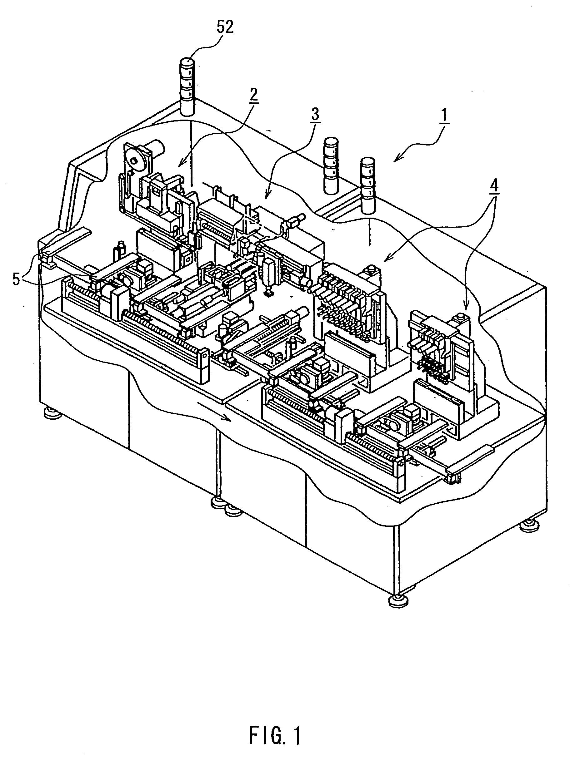
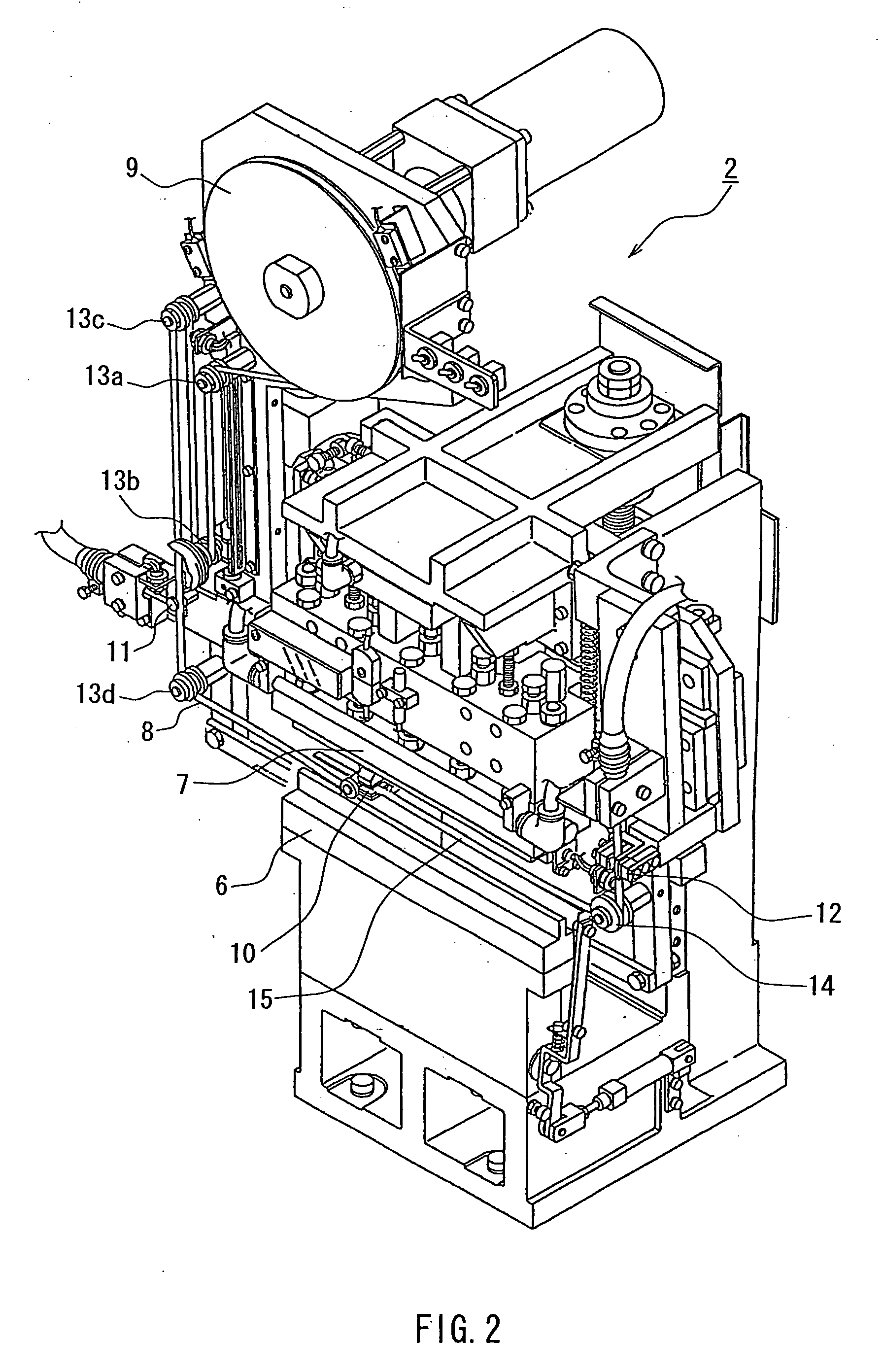
[0063]FIG. 1 is an oblique view of a component mounting device according to an embodiment of the present invention. The component mounting device 1 shown in this figure is a device that attaches ACF to a liquid crystal panel, which is the target object for attachment, and mounts a TCP, which is the mounted component. The component mounting device 1 includes an ACF attaching device 2. The ACF attaching device 2 attaches ACF to the liquid crystal panel, and peels off the ACF's release sheet. Then, the mounted component TCP is pre-pressured to the liquid crystal panel by a TCP pre-pressure portion 3, and the TCP is mounted onto the liquid crystal panel by a TCP actual-pressure portion 4.

[0064] Transport arms 5 are provided to transport the liquid crystal panel. A liquid crystal panel brought in from outside the device on the transport arms 5 is transported in the direction of the arrow while being passed to the next adjacent transport arms 5 when the operation in each of the portions ...

embodiment 2

[0092] Embodiment 1 was explained with an example in which it is judged whether or not the next single attachment unit can be ensured, but there is no limitation to this, and it is also possible to judge whether or not a length totaling the attachment lengths enough for all the ACF attachments on the next substrate can be ensured.

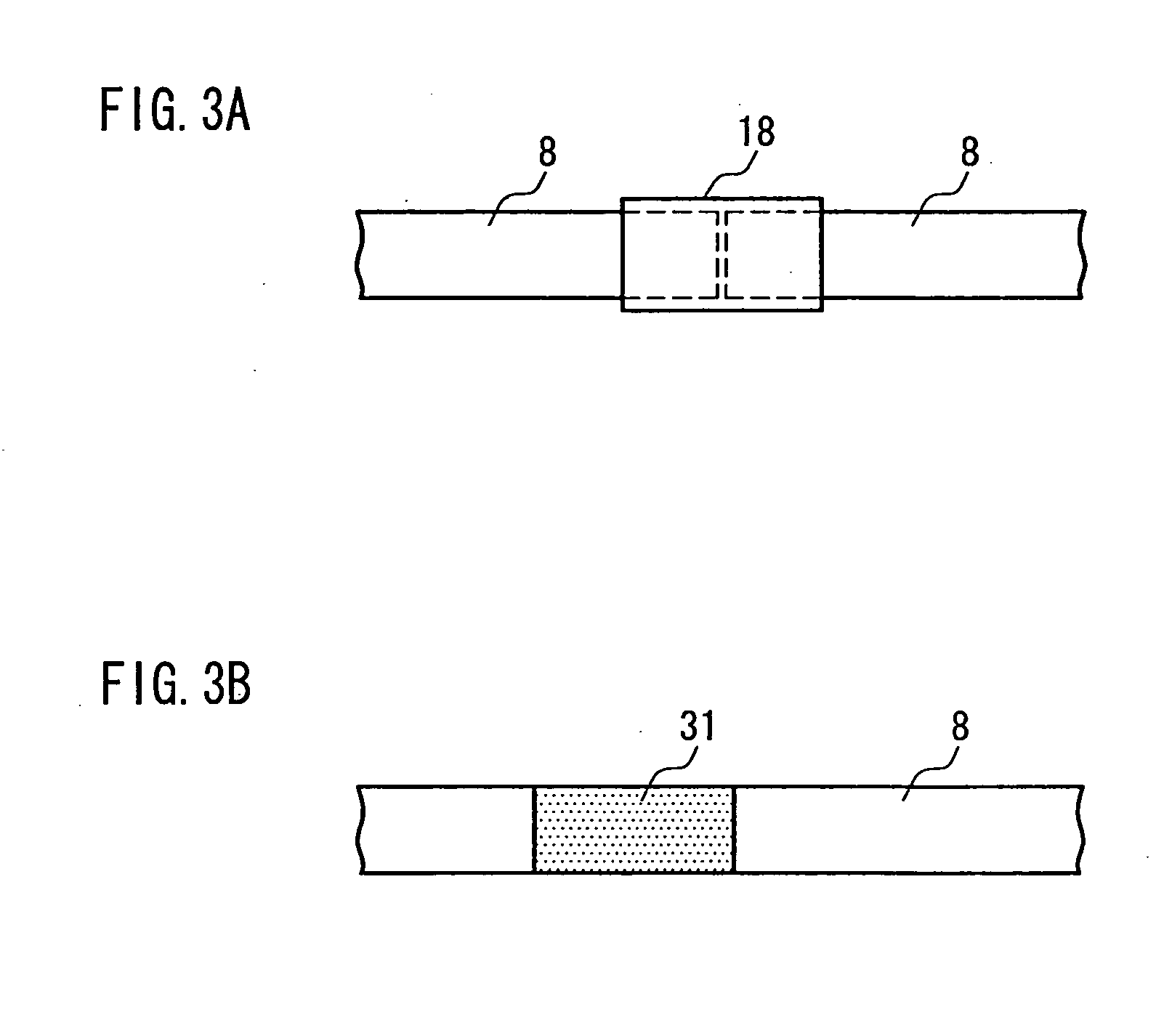
[0093] This embodiment will be explained with reference to FIG. 7. FIG. 7 shows a top view of an example substrate. A liquid crystal panel 17a is mounted on the substrate 17. The reference number 50 refers to the locations in which ICs for running the liquid crystal panel 17a are installed, that is, the locations in which ACFs are attached. In the example in FIG. 7, different single attachment units of ACF are to be attached in a total of three locations.

[0094] In this embodiment, when the joint 18 of the ACF is detected, it is judged whether or not enough ACF for the attachments of the current substrate 17 to which ACF is being attached can be ensured in...

embodiment 3

[0096]FIG. 8 is a process drawing of an ACF attaching device according to Embodiment 3. A step of cutting a final portion of the ACF 8 is carried out in this embodiment as in FIG. 6H, and the steps until the attaching of the final portion of the ACF 8 to the substrate are the same as in Embodiment 1. In this embodiment, an automatic skipping (forwarding through) of the joint 18 is performed when the joint 18 is detected.

[0097]FIG. 8A shows a state in which a sheet of a final portion of a single attachment unit of the ACF 8 has been attached after the joint 18 was detected by the joint sensor 11. With the chuck portion 10a in an open state, the feed chuck 10 moves in the direction of the arrow a, then stops before the cutter 16. The chuck portion 10a clamps and holds the release sheet 15. For convenience of explanation, the joint sensor 11 and the joint 18 are nearby in FIG. 8A, but FIG. 8A shows the state in which, after the joint sensor 11 detects the joint 18, the attachment of t...


PUM

PropertyMeasurementUnit
Lengthaaaaaaaaaa
Electrical conductoraaaaaaaaaa
Adhesivityaaaaaaaaaa

Abstract

An adhesive sheet attaching device is provided with: a stage (6); a feeder (10) for feeding adhesive sheet (8) onto the stage (6); a cutter (16); a pressurizer (7) for attaching the adhesive sheet (8) to a target object mounted on the stage (6); a detector (11) for detecting a connecting portion (18); and a controller. When the detector (11) detects the connecting portion (18), the controller stops the operation of the feeder (10) after adhesive sheet (8) of an attachable length up to the connecting portion (18) has been attached. This makes it possible to reliably prevent adhesive sheet (8) containing a connecting portion (18) from being attached to a target object, and to effectively use the adhesive sheet up to the connecting portion (18), thus making it possible to suppress resource loss.

Description

TECHNICAL FIELD [0001] The present invention relates to adhesive sheet attaching devices, adhesive sheet attaching methods, and component mounting devices, and to display panel production methods that use these, in which an adhesive sheet for fixing a mounted component is attached to a display panel such as a liquid crystal panel. BACKGROUND ART [0002] Conventionally, component mounting devices are known in which an adhesive sheet for fixing a mounted component is attached to a display panel such as a liquid crystal panel, and the mounted component is pressed onto the adhesive sheet. For example, there are electronic component mounting devices in which, after attaching ACF (anisotropic conductive film) with attached release sheet to a liquid crystal panel, and then peeling off the ACF's release sheet, a TCP (thin LSI-chip package) is pressed onto the ACF, and the TCP is mounted onto the liquid crystal panel. [0003]FIG. 12 shows process drawings of a conventional ACF attaching device...

Claims


Application Information

Patent Timeline
IPC IPC(8): B65H20/18H01L21/60B65H26/02B65H35/00G02F1/1345H05K3/32
CPCB65H20/18B65H26/02B65H35/0013B65H2511/162B65H2513/51B65H2220/01B65H2220/02Y02P80/30B65H2511/16G02F1/13
Inventor NISHIMOTO, TOMOTAKATSUJI, SHINJIROKATANO, RYOUICHIROU
Owner PANASONIC CORP
Why Eureka
Try Eureka