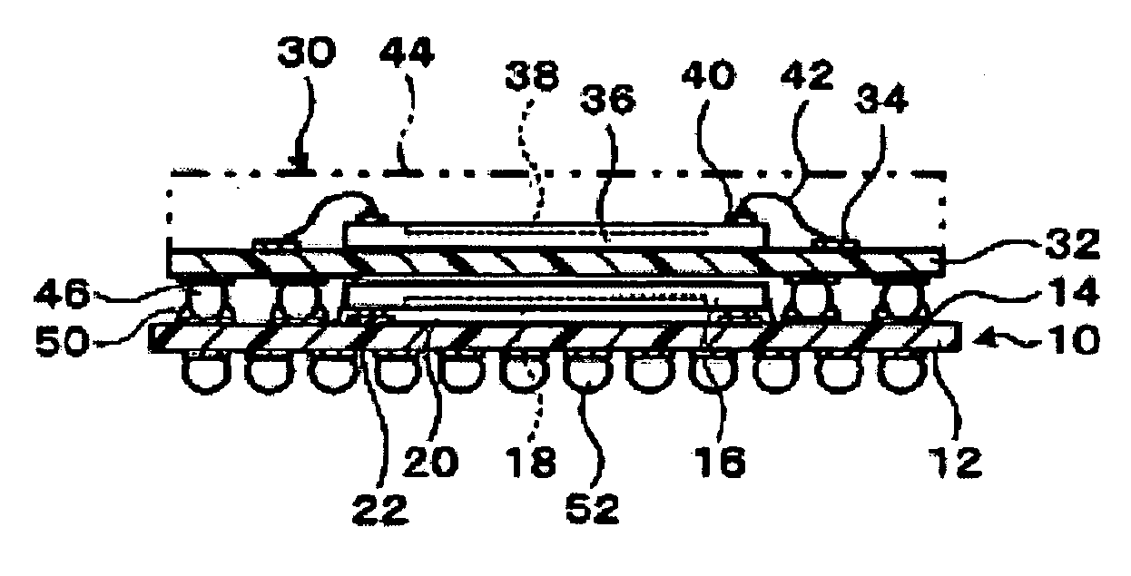
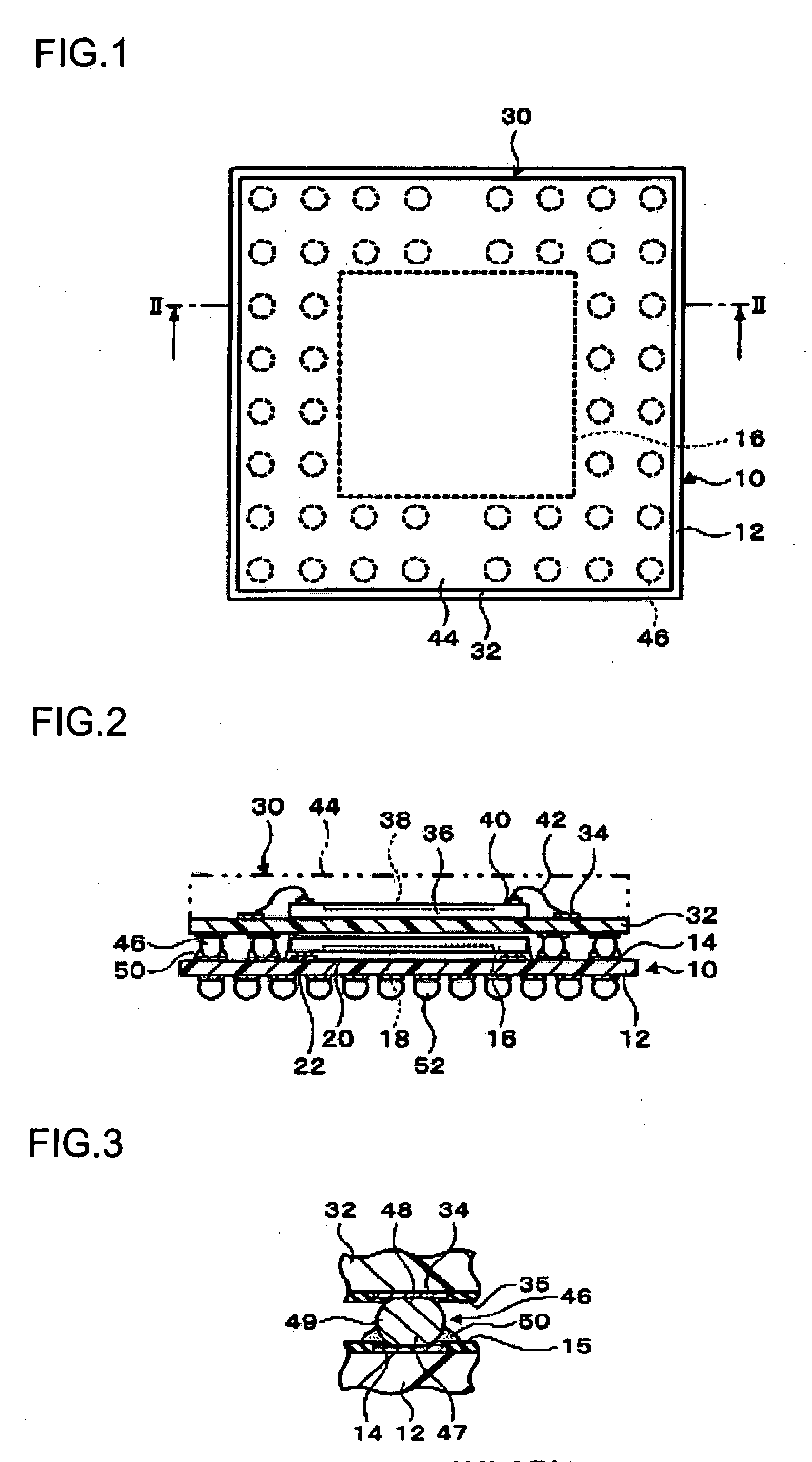
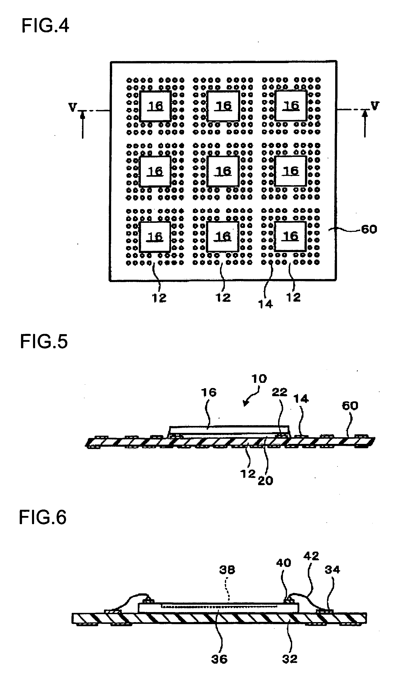
Semiconductor device, method for manufacturing the same, circuit board, and electronic equipment

Inactive Publication Date: 2005-12-01
SEIKO EPSON CORP
View PDF3 Cites 13 Cited by
  • Summary
  • Abstract
  • Description
  • Claims
  • Application Information

AI Technical Summary

Benefits of technology

[0007] A semiconductor device according to one aspect of the present invention comprises: a first package including a first interposer and a first semiconductor chip, the first interposer having a first wiring pattern, the first semiconductor chip being mounted on the first interposer and being electrically coupled to the first wiring pattern; a second package including a second interposer and a second semiconductor chip, the second interposer having a second wiring pattern, the second semiconductor chip being mounted on the second interposer and being electrically coupled to the second wiring pattern; a contact part electrically coupling the first wiring pattern to the second wiring pattern; and a reinforcer. A thermal expansion coefficient of the first package is larger than a thermal expansion coefficient of the second package. The second package is disposed so that the second interposer overlaps the first semiconductor chip and the first interposer. The contact part is provided between the first and second interposers so that a first end of the contact part is coupled to the first wiring pattern and a second end of the contact part is coupled to the second wiring pattern. The reinforcer is provided to expose a part of the contact part and cover circumference of the first end of the contact part. According to the present invention, the reinforcer covers the first end of the contact part, coupled to the first wiring patter. The first package having the first wiring pattern has a larger thermal expansion coefficient than the second package, and thus the rate of expansion when heated or contraction when cooled is larger. Therefore, larger stress is applied on the first end of the contact part, coupled to the first wiring patter. In the present invention, however, the contact part can be reinforced by the reinforcer effectively. Moreover, since part of the contact part is exposed through the reinforcer, space for releasing vapor and so on is formed between the first and second packages. This configuration can prevent the separation of the first and second packages due to the remaining of vapor and so on, allowing the improvement of bonding strength between the first and second interposes.
[0011] In the semiconductor device, the reinforcer may include flux. This configuration enhances the wettability of a solder material included in the contact part, for example, providing preferable electrical coupling between the contact part and the first wiring pattern.
[0013] In the semiconductor, the reinforcer may be a first reinforcer. The semiconductor device may further comprise a second reinforcer provided to expose a part of the contact part and cover circumference of the second end of the contact part. According to this, both ends of the contact part are covered by the first and second reinforcers with part of the contact part being exposed. Thus, the contact part can be reinforced more effectively.
[0016] A method for manufacturing a semiconductor device according to another aspect of the present invention, comprises: (a) mounting a first semiconductor chip on a first interposer having a first wiring pattern so that the first semiconductor chip is electrically coupled to the first wiring pattern, to form a first package; (b) mounting a second semiconductor chip on a second interposer having a second wiring pattern so that the second semiconductor chip is electrically coupled to the second wiring pattern, to form a second package; (c) disposing the second package so that the second interposer overlaps the first semiconductor chip and the first interposer; and (d) forming from a first material a contact part for electrically coupling the first wiring pattern to the second wiring pattern, and forming a reinforcer from a second material, between the first and second interposers. A thermal expansion coefficient of the first package is larger than a thermal expansion coefficient of the second package. A first end of the contact part is coupled to the first wiring pattern and a second end of the contact part is coupled to the second wiring pattern. In the step (d), the reinforcer is provided to expose a part of the contact part and cover circumference of the first end of the contact part. According to the present invention, the reinforcer is formed to cover the first end of the contact part, coupled to the first wiring patter. The first package having the first wiring pattern has a larger thermal expansion coefficient than the second package, and thus the rate of expansion when heated or contraction when cooled is larger. Therefore, larger stress is applied on the first end of the contact part, coupled to the first wiring patter. In the present invention, however, the contact part can be reinforced by the reinforcer effectively. Moreover, since part of the contact part is exposed through the reinforcer, space for releasing vapor and so on is formed between the first and second packages. This configuration can prevent the separation of the first and second packages due to the remaining of vapor and so on, allowing the improvement of bonding strength between the first and second interposes.
[0019] The method for manufacturing a semiconductor device, may further comprise prior to the step (d): providing the second material on the first and second interposers; and providing the first material on the second material on the first or second interposer. In the step (d), the reinforcer may be formed as a first reinforcer from the second material provided on the first interposer, and a second reinforcer may be formed from the second material provided on the second interposer. The second reinforcer exposes a part of the contact part and covers circumference of the second end of the contact part. According to this, both ends of the contact part are covered by the first and second reinforcers with part of the contact part being exposed. Thus, the contact part can be reinforced more effectively.

Problems solved by technology

However, if each semiconductor chip is supported by an interposer, the bonding strength between upper and lower interposers affects reliability.

Method used


Image

  • Semiconductor device, method for manufacturing the same, circuit board, and electronic equipment
  • Semiconductor device, method for manufacturing the same, circuit board, and electronic equipment
  • Semiconductor device, method for manufacturing the same, circuit board, and electronic equipment

Examples


first embodiment

[0038]FIG. 1 is a plan view illustrating a semiconductor device according to a first embodiment of the present invention. FIG. 2 is a sectional view of the semiconductor device shown in FIG. 1 along the line II-II. FIG. 3 is a partial enlarged view of FIG. 2.

[0039] The semiconductor device includes a first package 10. The first package 10 has a first interposer 12. The first interposer 12 is a substrate, and may be a plate. The first interposer 12 may be rectangular. The first interposer 12 may be made of a resin such as polyimide resin, or of a mixed material of organic (e.g. resin) and inorganic materials. Alternatively, the first interposer 12 may be a metal or ceramic substrate. The first interposer 12 is provided with a first wiring pattern 14. The first wiring pattern 14 may include a wire for electrically coupling a plurality of points, and a land electrically coupled to another part. The first wiring pattern 14 may be coved by an insulating layer 15, except for a certain pa...

second embodiment

[0065]FIG. 11 is a sectional view illustrating a semiconductor device according to a second embodiment of the present invention. In the present embodiment, a semiconductor device has a first reinforcer 70 and a second reinforcer 72.

[0066] The first and second reinforcers 70 and 72 are provided between the first and second interposers 12 and 32. The first and second reinforcers 70 and 72 are provided with part of the contact part 46 being exposed. The description of exposed part of the contact part 46 is as above.

[0067] The first reinforcer 70 covers a first end of the contact part 46, coupled to the first wiring pattern 14. The details of the first reinforcer 70 are the same as the above description of the reinforcer 50.

[0068] The second reinforcer 72 covers a second end of the contact part 46, coupled to the second wiring pattern 34. The second reinforcer 72 is provided while avoiding the first interposer 12 (not in contact with the first interposer 12). The second reinforcer 72...


PUM


Abstract

A semiconductor device includes a first package, a second package, a contact part for electrically coupling a first wiring pattern to a second wiring pattern, and a reinforcer. The thermal expansion coefficient of the first package is larger than that of the second package. The second package is disposed so that the second interposer overlaps the first semiconductor chip and the first interposer. The contact part is provided between the first and second interposers so that a first end is coupled to the first wiring pattern and a second end is coupled to the second wiring pattern. The reinforcer is provided to expose part of the contact part and cover the circumference of the first end of the contact part.

Description

RELATED APPLICATIONS [0001] This application claims priority to Japanese Patent Application No. 2004-156268 filed May 26, 2004 which is hereby expressly incorporated by reference herein in its entirety. BACKGROUND [0002] 1. Technical Field [0003] The present invention relates to a semiconductor device, a method for manufacturing the same, a circuit board, and electronic equipment. [0004] 2. Related Art [0005] Stacked semiconductor devices have been developed. Since semiconductor chips in the devices are mounted three dimensionally, reducing two-dimensional space required. Furthermore, the device can be formed by combining existing semiconductor chips and thus do not require new design for integrated circuits. However, if each semiconductor chip is supported by an interposer, the bonding strength between upper and lower interposers affects reliability. If any moisture remains in between upper and lower interposers, it can turn into vapor and expand through high-temperature reflow pro...

Claims


Application Information

Patent Timeline
IPC IPC(8): H01L25/18H01L21/48H01L23/31H01L23/52H01L25/065H01L25/07H01L25/10
CPCH01L23/3128H01L24/97H01L2224/48091H01L2224/48227H01L2224/73204H01L2924/15311H01L2924/15331H01L25/105H01L2224/97H01L2924/07802H01L2225/1058H01L2225/1023H01L2224/16225H01L24/48H01L2224/32225H01L2224/73265H01L2924/00014H01L2924/00012H01L2924/00H01L2224/85H01L24/73H01L2224/48465H01L2924/14H01L2924/15787H01L2924/181H01L2224/81H01L2224/45099H01L2224/45015H01L2924/207
Inventor AOYAGI, AKIYOSHI
Owner SEIKO EPSON CORP
Why Eureka
Try Eureka