Illuminating device for photographing and camera

a technology of illumination device and illumination device, which is applied in the direction of color television details, television systems, instruments, etc., can solve the problems of not disclosing the technology of intentionally non-uniform illumination within the image plane, uneven illumination of the subject, etc., and achieve the effect of minimizing the extent of uneven illumination

Active Publication Date: 2005-12-01
NIKON CORP
View PDF2 Cites 95 Cited by
  • Summary
  • Abstract
  • Description
  • Claims
  • Application Information

AI Technical Summary

Benefits of technology

[0023] According to the 11th aspect of the invention, in the illuminating device for photographing according to the 9th aspect, it is preferred that: there is further provided a prohibiting unit that prohibits light emission at the second illuminating unit, at least if a subject distance is equal to or less than a predetermined value, if sensitivity is equal to or greater than a predetermined value, or if an aperture value is set toward an open side relative to a predetermined value; and while the light emission at the second illuminating unit is prohibited by the prohibiting unit, the light emission control unit controls the light emission at the plurality of light emitting elements in the first illuminating unit by using the light emission brightness information stored in the storage unit so as to minimize an extent of uneven illumination of the subject attributable to the first illuminating unit.

Problems solved by technology

The quantity of illuminating light emitted from a single LED is normally smaller than the quantity of illuminating light provided by a discharge-type illuminating device such as a xenon discharge tube, and for this reason, the brightness of the subject illuminated with LEDs disposed in a simple dispersive arrangement may become uneven, i.e., uneven illumination may occur.
While it is described in Japanese Laid Open Patent Publication No. 2002-207236 that shadowing of the subject can be eliminated and the overall quantity of illuminating light can be increased by fitting the illuminating device with a plurality of LEDs, the publication does not disclose that a technology for achieving intentionally nonuniform brightness within the image plane.
There is also a problem with the method in which the light emitting element is mechanically moved in that the operation for adjusting the illuminating angle becomes a time-consuming procedure.

Method used


Image

  • Illuminating device for photographing and camera
  • Illuminating device for photographing and camera
  • Illuminating device for photographing and camera

Examples


first embodiment

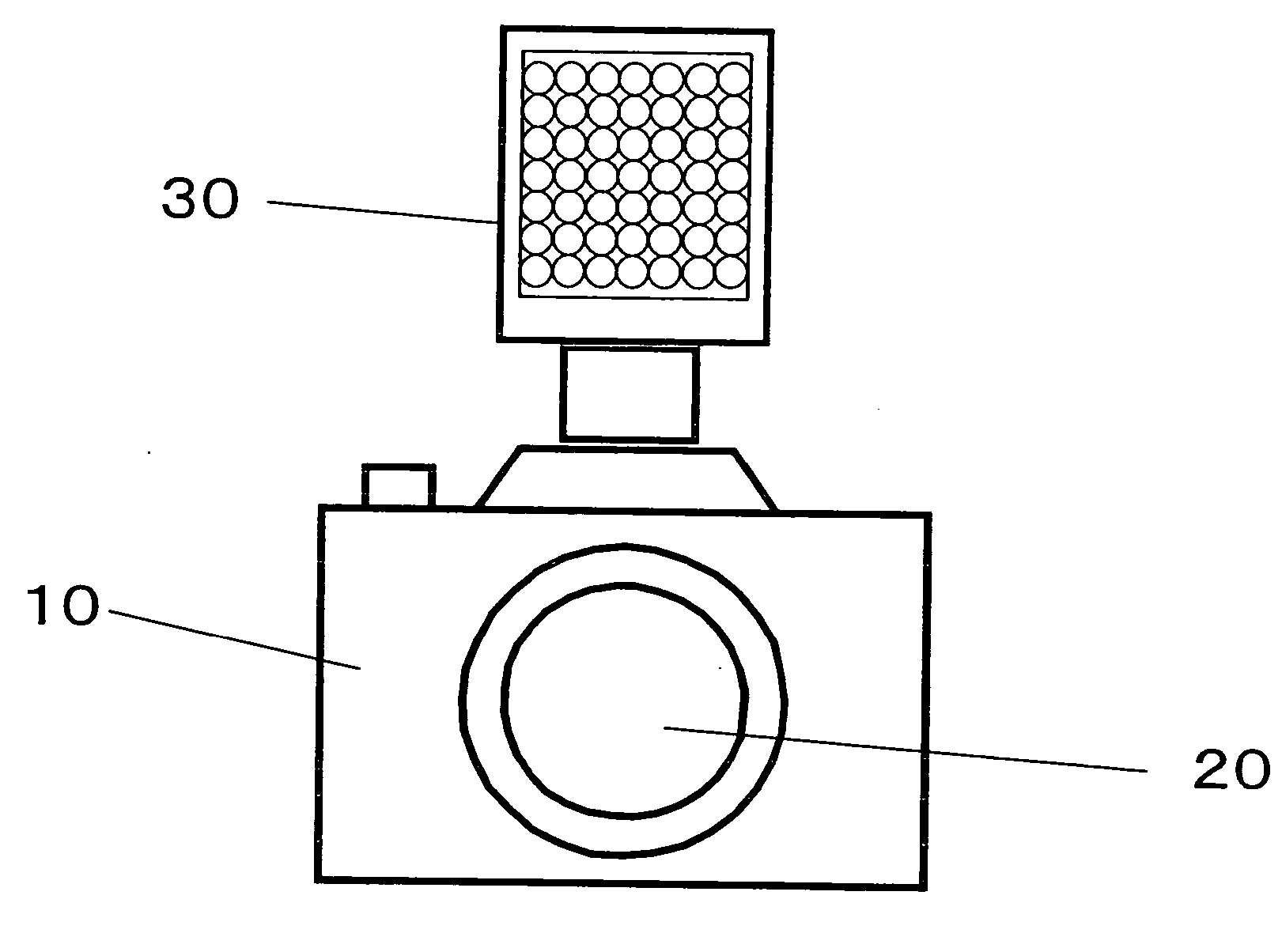
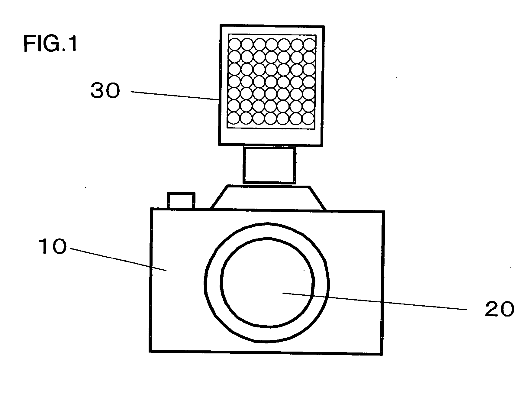
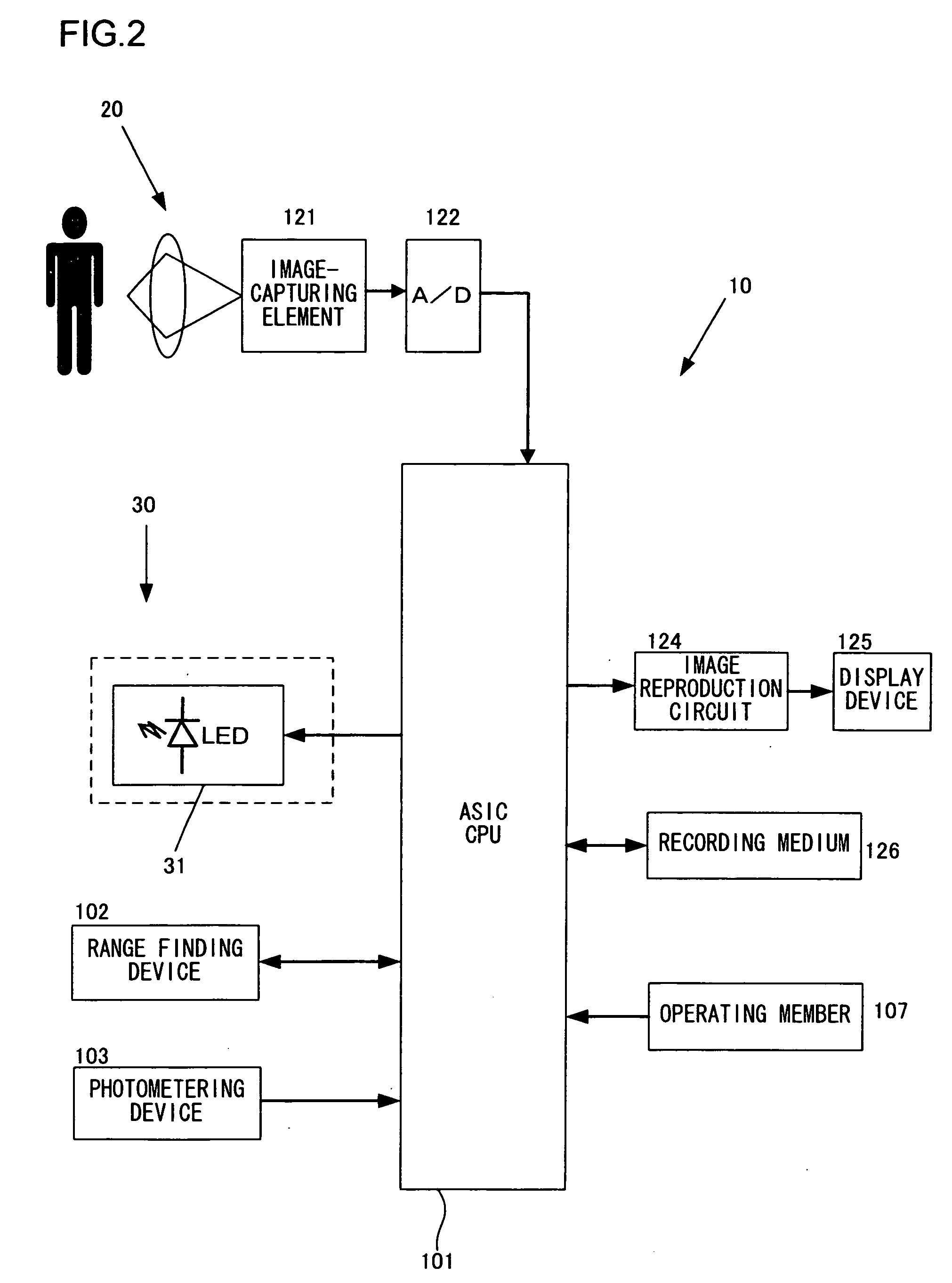
[0066] The following is an explanation of a preferred embodiment of the present invention, given in reference to drawings. FIG. 1 shows the electronic camera system achieved in the first embodiment of the present invention. As illustrated in FIG. 1, an interchangeable photographic lenses 20 is mounted at an electronic camera body 10. An illuminating device (or a lighting device) 30 is mounted at an accessory shoe (not shown) of the electronic camera 10.

[0067]FIG. 2 is a block diagram showing the essential structure adopted in the electronic camera system in FIG. 1. The illuminating device 30 shown in FIG. 2 includes a light emission circuit 31 that engages LEDs (light emitting diodes) in light emission. The illuminating device 30 engages in communication with a CPU 101 at the camera body 10 via a communication contact point (not shown) present at the accessory shoe to receive timing signals provided as instructions for the LEDs to start and end light emission, a signal indicating t...

second embodiment

[0116] Uneven illumination by a discharge type illuminating device such as a xenon (Xe) discharge tube may be corrected through the processing executed to correct the difference in the brightness in the central area and the peripheral area within the angle of view as explained earlier. FIG. 6 shows an example of a structure that may be adopted in the light emission circuit in the illuminating device 30 achieved in the second embodiment. The light emission circuit in FIG. 6 includes a DC / DC converter 201, a voltage detection circuit 202, a main capacitor 203, a light emission control circuit 204, a current supply circuit 205, a flash control / voltage boost / brightness control circuit 206, an interface circuit 207, a xenon tube 209 and a group of LEDs 210.

[0117] The DC / DC converter 201 boosts (e.g., to 300V) the voltage supplied from the battery 1 and charges the main capacitor 203. The voltage detection circuit 202 detects the charge voltage at the main capacitor 203 and outputs a det...

third embodiment

[0131]FIG. 9 shows a camera system that includes the illuminating device achieved in the third embodiment of the present invention. As shown in FIG. 9, an illuminating device 320 is mounted at an accessory shoe (not shown) of a camera 310.

[0132]FIG. 10 is a block diagram of the essential the structure adopted in the illuminating device 320. The illuminating device 320 includes a CPU 401, a display information generating circuit 402, a display device 403, a nonvolatile memory 404, an operating member 405 and a light emission circuit 321 that engages LEDs (light emitting diodes) in light emission.

[0133] The CPU 401 is constituted with an ASIC or the like. The CPU 401 executes specific arithmetic operations by using signals input thereto from various blocks and outputs control signals generated based upon the arithmetic operation results to the individual blocks. In addition, the CPU 401 includes an interface circuit (not shown) which is used to engage in communication with a CPU on ...


PUM


Abstract

An illuminating device for photographing includes: an illuminating unit having a plurality of current-controlled light emitting elements, which illuminates a subject with light emitted from the plurality of light emitting elements; a storage unit in which light emission brightness information is stored in correspondence to each of the plurality of light emitting elements; and a light emission control unit that controls light emission at the plurality of light emitting elements based upon the light emission brightness information stored in the storage unit so that the plurality of light emitting elements achieve uniform brightness levels at the subject.

Description

INCORPORATION BY REFERENCE [0001] The disclosures of the following priority applications are herein incorporated by reference: [0002] Japanese Patent Application No. 2004-154999 filed May 25, 2004 [0003] Japanese Patent Application No. 2004-183594 filed Jun. 22, 2004 [0004] Japanese Patent Application No. 2004-183595 filed Jun. 22, 2004 BACKGROUND OF THE INVENTION [0005] 1. Field of the Invention [0006] The present invention relates to an illuminating device that illuminates a subject during a photographing operation and a camera. [0007] 2. Description of Related Art [0008] There is a camera known in the related art that illuminates a main subject with an illuminating device having a plurality of LEDs (see Japanese Laid Open Patent Publication No. 2002-207236). Japanese Laid Open Patent Publication No. 2002-207236 discloses a technology for preventing a shadow from being cast on one side of the subject due to illuminating light being emitted from a single position by distributing th...

Claims


Application Information

Patent Timeline
Patent Type & Authority Applications(United States)
IPC IPC(8): G03B15/02G03B15/05H04N5/225H04N5/235
CPCG03B15/05H04N5/2354H04N5/2256G03B2215/0567G03B2215/0571H04N23/56H04N23/74
Inventor MATSUIHOSHUYAMA, HIDEOTAKEMOTO, MASAMI
Owner NIKON CORP
Why Eureka
Try Eureka