Aperiodic dielectric multilayer stack

a dielectric and multi-layer technology, applied in the direction of layered products, semiconductor lasers, transportation and packaging, etc., can solve the problems of large surface area, difficult and expensive production, and difficult production of efficient crystalline-based devices, and achieve the effect of substantial differences in thickness

Active Publication Date: 2005-12-01
THE TRUSTEES FOR PRINCETON UNIV
View PDF22 Cites 163 Cited by
  • Summary
  • Abstract
  • Description
  • Claims
  • Application Information

AI Technical Summary

Benefits of technology

[0013] A structure is provided that includes an aperiodic dielectric stack. The structure may include a substrate, a device disposed over the substrate, and a first dielectric stack disposed between the substrate and the device. The first dielectric stack includes a plurality of layers comprising a first dielectric material, wherein at least two of the layers comprising a first dielectric material have substantially different thicknesses, as well as a plurality of layers comprising a second dielectric material. The average outcoupling efficiency into air of the device over a bandwidth of at least 300 nm may be at least 40% greater than that of an otherwise identical device disposed in a structure without the first dielectric stack. The substrate may have a treated surface such that light that may

Problems solved by technology

However, efficient crystalline-based devices, especially of large surface area, are difficult and expensive to produce due to the cost and difficulty inherent in producing large crystals

Method used


Image

  • Aperiodic dielectric multilayer stack
  • Aperiodic dielectric multilayer stack
  • Aperiodic dielectric multilayer stack

Examples


Embodiment Construction

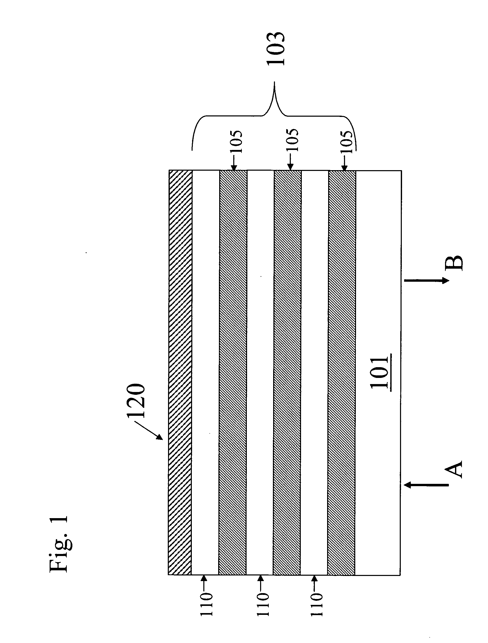
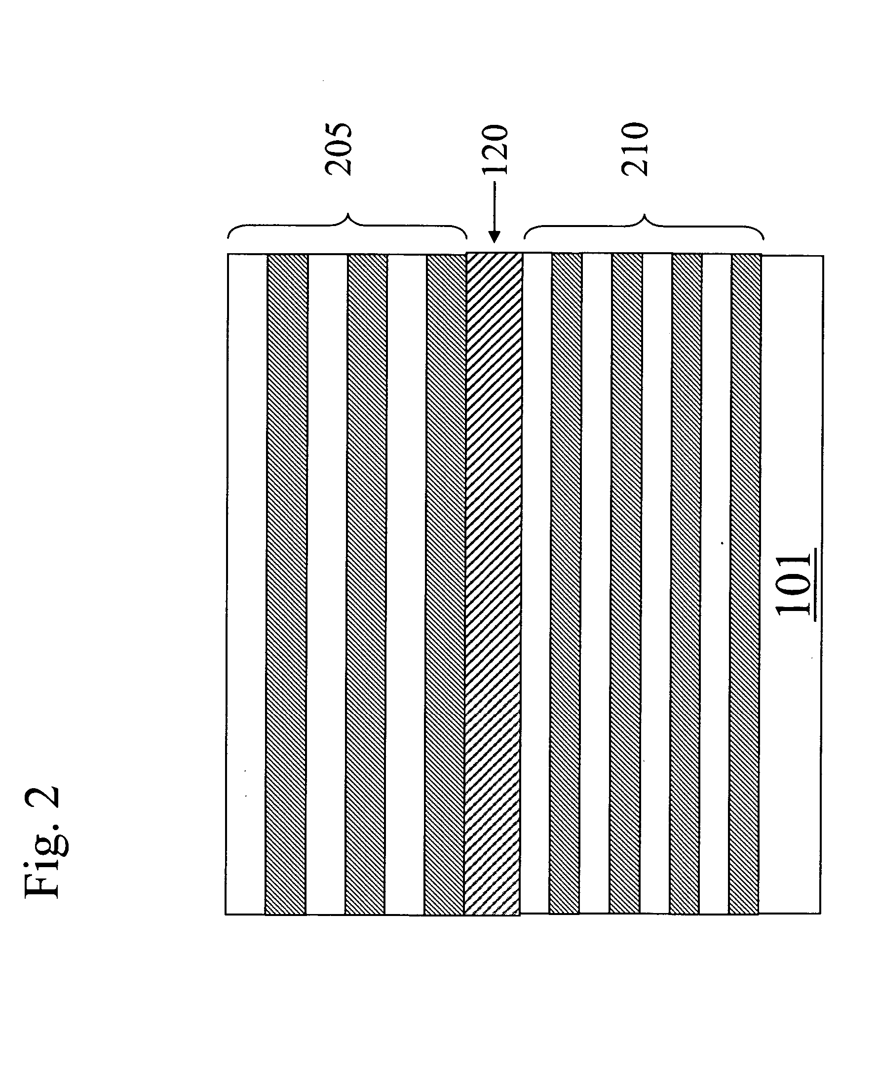
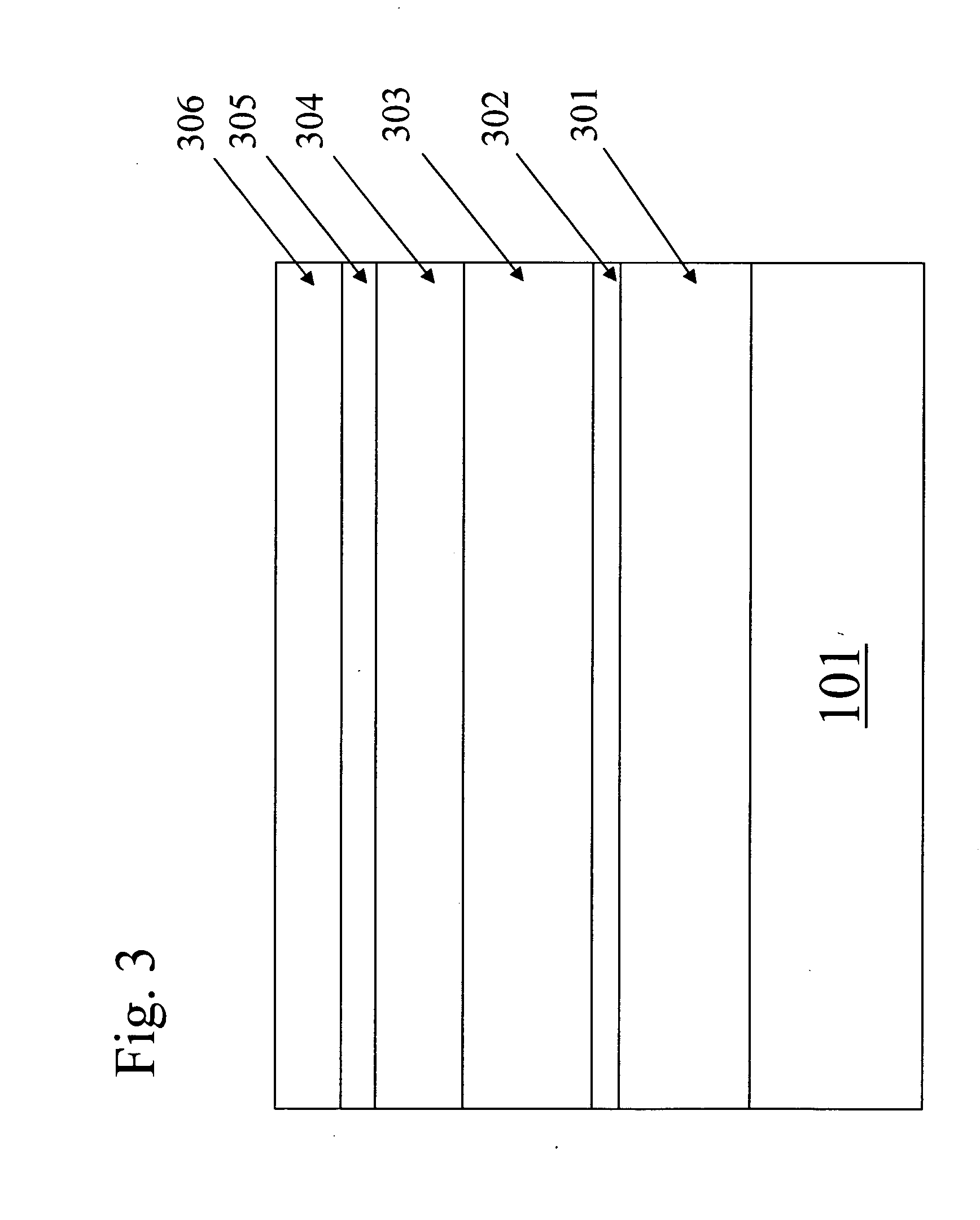
[0026] The photoresponse of organic PV cells with a well-defined layer structure can be accurately predicted by modeling the optical properties of the multilayer stack while simultaneously solving for exciton diffusion. Using aperiodic multilayer stacks, significant light coupling improvements may be realized, for example, a broad increase in coupling of light across the visible spectrum may be realized. Thin layer optoelectronic devices, designed for optimal diffusion efficiency, may suffer losses in, for example, absorption efficiency due to the thinness of the components. Aperiodic dielectric multilayer mirrors may be designed that have a reasonable reflectivity and a tailored phase behavior. Therefore, when these mirrors are used in combination with, for example, thin layer devices, gains in, for example, absorption efficiency and external quantum efficiency may be achieved. For example, a stack may be designed that would allow normally incident photons, or photons within a cert...


PUM


Abstract

A structure is provided that includes an aperiodic dielectric stack. The structure may include a substrate, a device disposed over the substrate, and a first dielectric stack disposed between the substrate and the device. The first dielectric stack includes a plurality of layers comprising a first dielectric material, wherein at least two of the layers comprising a first dielectric material have substantially different thicknesses, as well as a plurality of layers comprising a second dielectric material. The average outcoupling efficiency into air of the device over a bandwidth of at least 300 nm may be at least 40% greater than that of an otherwise identical device disposed in a structure without the first dielectric stack. The substrate may have a treated surface such that light that may otherwise be waveguided in the substrate is outcoupled into air, and the average outcoupling efficiency into air of the device over a bandwidth of at least 300 nm may be at least 10% greater than that of an otherwise identical device disposed in a structure without the first dielectric stack. The structure may include an optical cavity defined by a first end layer and a second end layer, where the first end layer further comprising a first dielectric stack having a plurality of layers comprising a first dielectric material, wherein at least two of the layers comprising a first dielectric material have substantially different thicknesses, and a plurality of layers comprising a second dielectric material. An optoelectronic device having a first active layer may be disposed within the optical cavity.

Description

FIELD OF THE INVENTION [0001] The present invention relates to the use of optoelectronic devices, and more specifically to optimized aperiodic dielectric multilayer stacks for use with optoelectronic devices, such as OLEDs and photovoltaic cells. BACKGROUND [0002] Optoelectronic devices rely on the optical and electronic properties of materials to either produce or detect electromagnetic radiation electronically or to generate electricity from ambient electromagnetic radiation. Photosensitive optoelectronic devices convert electromagnetic radiation into electricity. Photovoltaic (PV) devices or solar cells, which are a type of photosensitive optoelectronic device, are specifically used to generate electrical power. PV devices, which may generate electrical power from light sources other than sunlight, are used to drive power consuming loads to provide, for example, lighting, heating, or to operate electronic equipment such as computers or remote monitoring or communications equipmen...

Claims


Application Information

Patent Timeline
IPC IPC(8): H01L51/52H01S5/00
CPCY10T428/24975H01L51/5265H10K50/852
Inventor PEUMANS, PETERFORREST, STEPHEN
Owner THE TRUSTEES FOR PRINCETON UNIV
Why Eureka
Try Eureka