Vertical field effect transistors incorporating semiconducting nanotubes grown in a spacer-defined passage

a technology of semiconducting nanotubes and vertical field effect transistors, which is applied in the direction of nanotechnology, semiconductor devices, electrical apparatus, etc., can solve the problems of large variation in current flowing from the source to the drain, and the incompatibility of horizontal fet device structures with mass production techniques, so as to achieve efficient and effective introduction

Inactive Publication Date: 2005-12-01
IBM CORP
View PDF9 Cites 33 Cited by
  • Summary
  • Abstract
  • Description
  • Claims
  • Application Information

AI Technical Summary

Benefits of technology

[0009] Consistent with the principles of the invention, nanotube growth is constrained to a well-defined vertical growth direction inside a high-aspect ratio open space or passage defined by a spacer adjacent to the gate electrode. As a result, the conventional difficulty associated with the isotropic directional growth of nanotubes is eliminated. A gap may be provided in the spacer that permits efficient and effective introduction of the reactant or reactants required to grow the carbon nanotubes into the passage in the vicinity of the interface region between the catalyst material and each growing nanotube. The length of the channel region between the source and drain is defined by the vertical dimension or thickness of the gate electrode without the limitations imposed by conventional lithographic processes used in semiconductor device fabrication. As a result, the length of the channel region may have a feature size that is smaller than feature sizes produced by standard lithographic and etch processes.

Problems solved by technology

A small change in gate voltage can cause a large variation in the current flowing from the source to the drain.
Although successfully formed under laboratory conditions by manipulating single carbon nanotubes using an atomic force microscope, these horizontal FET device structures are incompatible with mass production techniques.

Method used


Image

  • Vertical field effect transistors incorporating semiconducting nanotubes grown in a spacer-defined passage
  • Vertical field effect transistors incorporating semiconducting nanotubes grown in a spacer-defined passage
  • Vertical field effect transistors incorporating semiconducting nanotubes grown in a spacer-defined passage

Examples


Embodiment Construction

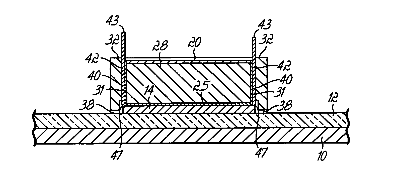
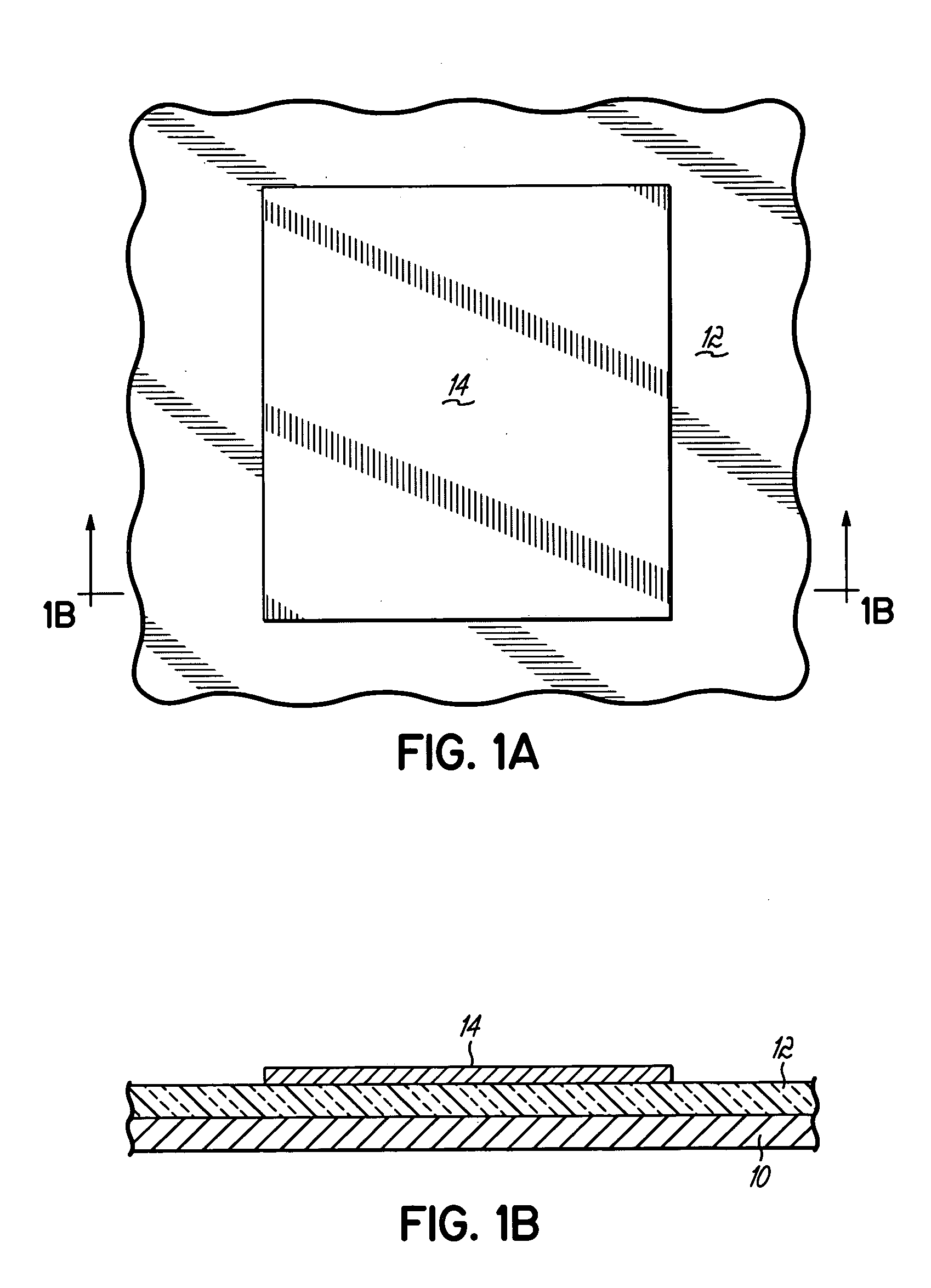
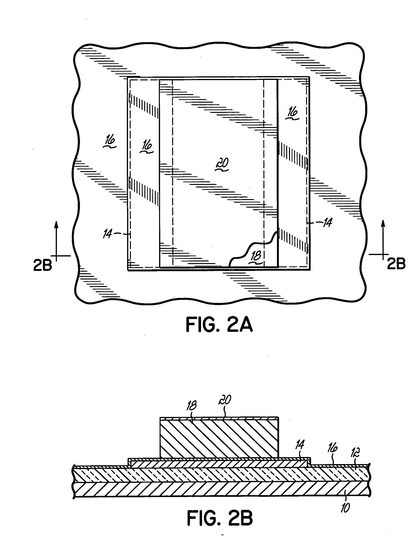
[0037] The invention is directed to vertical field effect transistors (FET's) that utilize carbon nanotubes as a semiconducting material for the channel region providing a selective conduction path between a source and a drain. In accordance with the principles of the invention, the carbon nanotubes are grown in a confined vertical open space or passage such that isotropic growth is prevented. As a result, the carbon nanotubes are substantially vertically oriented and situated in a desired location adjacent to a gate electrode to which voltage is applied for controlling the current flowing from the source to the drain. The length of the channel region between the source and drain is defined by the thickness of the gate electrode, which is substantially equal to the nanotube length, and is not dependent upon a lithographic process. The nanotube growth rate is enhanced by providing an additional flow pathway for gaseous or vaporized reactants to a catalytic material residing at the ba...


PUM


Abstract

Vertical field effect transistors having a channel region defined by at least one semiconducting nanotube and methods for fabricating such vertical field effect transistors by chemical vapor deposition using a spacer-defined channel. Each nanotube is grown by chemical vapor deposition catalyzed by a catalyst pad positioned at the base of a high-aspect-ratio passage defined between a spacer and a gate electrode. Each nanotube grows in the passage with a vertical orientation constrained by the confining presence of the spacer. A gap may be provided in the base of the spacer remote from the mouth of the passage. Reactants flowing through the gap to the catalyst pad participate in nanotube growth.

Description

CROSS-REFERENCE TO RELATED APPLICATIONS [0001] This application is a divisional of U.S. patent application Ser. No. 10 / 767,039, filed Jan. 29, 2004, the disclosure of which is hereby incorporated by reference herein in its entirety.FIELD OF THE INVENTION [0002] The invention relates to semiconductor device fabrication and, more particularly, to vertical field effect transistors incorporating semiconducting nanotubes as a channel region and methods of fabricating such vertical field effect transistors. BACKGROUND OF THE INVENTION [0003] Traditional field effect transistors (FET's) are familiar conventional devices commonly incorporated as a fundamental building block into the intricate circuitry of integrated circuit (IC) chips. A single IC chip may feature many thousands to millions of FET's, along with other passive components such as resistors and capacitors, interconnected by conductive paths. FET's operate by varying the resistivity of a channel in a channel region separating a ...

Claims


Application Information

Patent Timeline
Patent Type & Authority Applications(United States)
IPC IPC(8): H01L21/78H01L27/28H01L51/30
CPCB82Y10/00H01L27/283H01L51/0048Y10S977/707Y10S977/70Y10S977/724Y10S977/721H01L51/057H10K19/10H10K85/221H10K10/491H01L21/18B82Y40/00H10K10/00
Inventor FURUKAWA, TOSHIHARUHAKEY, MARK CHARLESHOLMES, STEVEN JOHNHORAK, DAVID VACLAVMITCHELL, PETER H.NESBIT, LARRY ALAN
Owner IBM CORP
Why Eureka
Try Eureka