Method of forming nitrogen and phosphorus doped amorphous silicon as resistor for field emission display device baseplate

a technology of resistor and amorphous silicon, which is applied in the manufacture of electrode systems, electric discharge tubes/lamps, and discharge tubes luminescnet screens, etc., can solve the problems of short circuit of the device, short circuit of the resistor layer, and nucleation related defects at the interface of the resistor and metal, so as to reduce the nucleation problem and be less mobile

Inactive Publication Date: 2005-12-01
MICRON TECH INC
View PDF16 Cites 0 Cited by
  • Summary
  • Abstract
  • Description
  • Claims
  • Application Information

AI Technical Summary

Benefits of technology

[0011] Briefly stated, the needs addressed above are solved by providing an amorphous silicon resistor layer doped with nitrogen and phosphorus over a metallic layer of aluminum, chromium, or both. For instance, in an FED structure having either a metallic layer of aluminum or a chromium / aluminum bilayer, a nitrogen-phosphorous-doped silicon resistor layer is deposited over the metal. The use of nitrogen-doped silicon solves the problems stated above because the N—Si bond is longer and stronger than the B—Si bond. Therefore, Si is less likely to diffuse out of the resistor layer into the aluminum to cause short-circuiting. Furthermore, the strength of the N—Si bond makes the atoms in the resistor layer less mobile, thereby diminishing the nucleation problem at the resistor / metal interface.

Problems solved by technology

One problem with FEDs has been the shorting of the resistor layer.
Short-circuiting of the device may occur in this structure because of diffusion of silicon from the resistor layer into the metal at temperatures above about 300° C. This problem is especially prevalent when the resistor layer is deposited directly over an aluminum layer.
Diffusion of silicon into the aluminum will take place, for instance, during deposition at temperatures from about 330 to 400° C., or during packaging of the baseplate at temperatures of about 450° C. This diffusion problem is caused primarily because Si forms a eutectic contact with Al above 400° C., and also because the free energy of silicon is higher in its amorphous state.
Another problem is that resistor layers made of boron-doped amorphous silicon cause nucleation related defects at the interface of the resistor and metal, especially when the metal is chromium.
In an FED structure using a chromium metallic layer, for instance, the interaction of diborane gas at the chromium surface causes irregularities at the surface between the metal and resistor.
Discontinuities in the resistor layer can cause the loss of the benefits for which the resistor layer was used in the first place.
Additionally, discontinuities in the resistor layer can present problems when subsequent etching or photolithographic processes are conducted, potentially causing delamination of various layers and other irregularities.

Method used


Image

  • Method of forming nitrogen and phosphorus doped amorphous silicon as resistor for field emission display device baseplate
  • Method of forming nitrogen and phosphorus doped amorphous silicon as resistor for field emission display device baseplate
  • Method of forming nitrogen and phosphorus doped amorphous silicon as resistor for field emission display device baseplate

Examples


Embodiment Construction

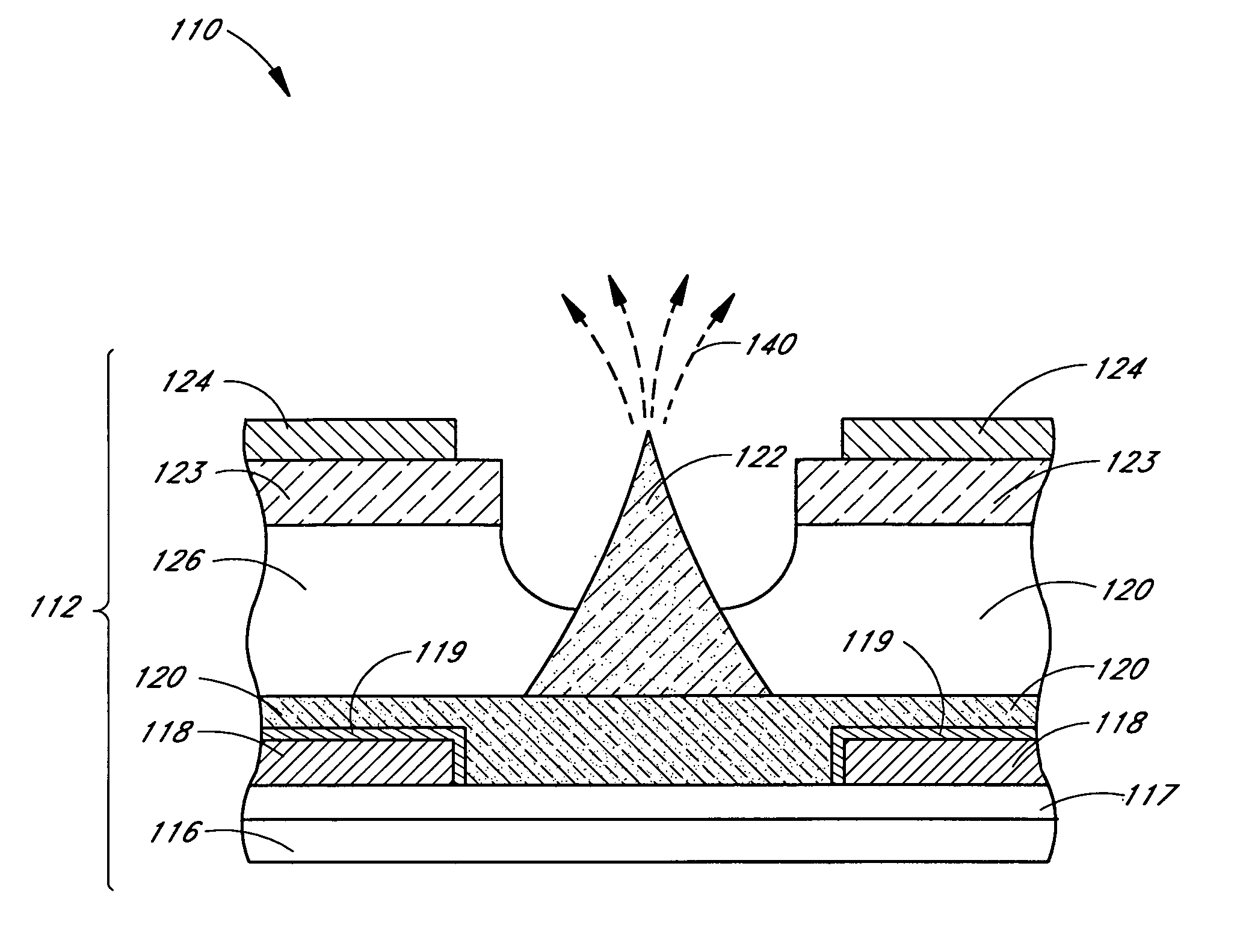
[0021] The preferred embodiments are field emission display devices having a resistor that eliminates short circuiting of the device. It will be appreciated that although the preferred embodiments are described with respect to FED devices, the methods and apparatus taught herein are applicable to other devices where it is desired to eliminate short-circuiting and defect-related problems between a resistor-type layer and a metallic layer.

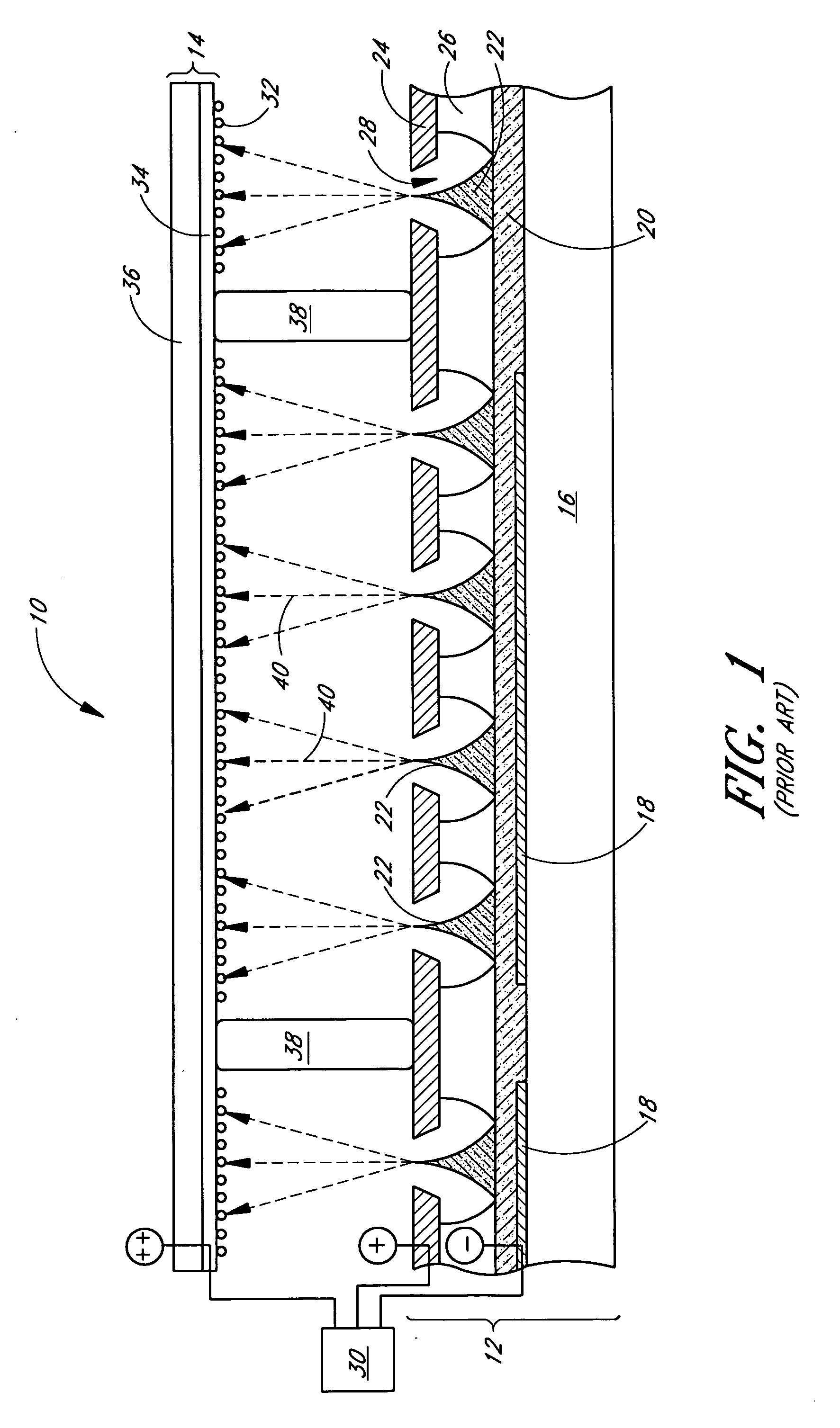
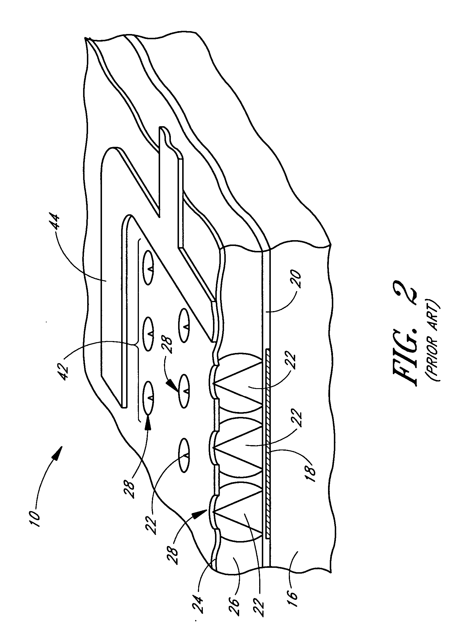
[0022]FIG. 1 illustrates a portion of a conventional flat panel display, including a plurality of field emission devices. Flat panel display 10 comprises a baseplate 12 and a faceplate 14. Baseplate 12 includes substrate 16, which is preferably formed from an insulative glass material. Column interconnects 18 are formed and patterned over substrate 16. The purpose and function of column interconnects 18 is disclosed in greater detail below. Furthermore, a resistor layer 20, which is also discussed in greater detail below, may be disposed over column...


PUM

PropertyMeasurementUnit
temperaturesaaaaaaaaaa

Abstract

Described herein is a resistor layer for use in field emission display devices and the like, and its method of manufacture. The resistor layer is an amorphous silicon layer doped with nitrogen and phosphorus. Nitrogen concentration in the resistor layer is preferably between about 5 and 15 atomic percent. The presence of nitrogen and phosphorus in the silicon prevents diffusion of Si atoms into metal conductive layers such as aluminum, even up to diffusion and packaging temperatures. The nitrogen and phosphorus also prevent defects from forming at the boundary between the resistor layer and metal conductor. This leads to better control over shorting and improved resistivity in the resistor.

Description

RELATED APPLICATIONS [0001] This application is a continuation of U.S. patent application Ser. No. 10 / 644,443, filed Aug. 19, 2003, now U.S. Pat. No. 6,911,766, which is a continuation of U.S. patent application Ser. No. 09 / 388,697, filed Sep. 2, 1999, now U.S. Pat. No. 6,635,983. The disclosure of the aforementioned patents is incorporated herein by reference in their entirety.REFERENCE TO GOVERNMENT CONTRACT [0002] This invention was made with United States Government support under Contract No. DABT63-97-C-0001, awarded by the Advanced Research Projects Agency (ARPA). The United States Government has certain rights in this invention.BACKGROUND OF THE INVENTION [0003] 1. Field of the Invention [0004] This invention relates to a resistor layer for a field emission device and the like, and more particularly, to a resistor layer that prevents shorting in a field emission display baseplate. [0005] 2. Description of the Related Art [0006] A field emission device (FED) typically includes...

Claims


Application Information

Patent Timeline
Patent Type & Authority Applications(United States)
IPC IPC(8): H01J1/02H01J1/304H01J1/62H01J9/02H01J19/02H01J63/04
CPCH01J1/30H01J1/304H01J1/3044H01J2329/00H01J31/127H01J2201/319H01J9/025
Inventor RAINA, KANWAL K.MORADI, BENHAM
Owner MICRON TECH INC
Why Eureka
Try Eureka