Semiconductor memory device having first and second memory cell arrays and a program method thereof
a memory cell array and memory technology, applied in the field of semiconductor memory devices, can solve problems such as difficulty in reducing the cell area
- Summary
- Abstract
- Description
- Claims
- Application Information
AI Technical Summary
Problems solved by technology
Method used
Image

Examples
first embodiment
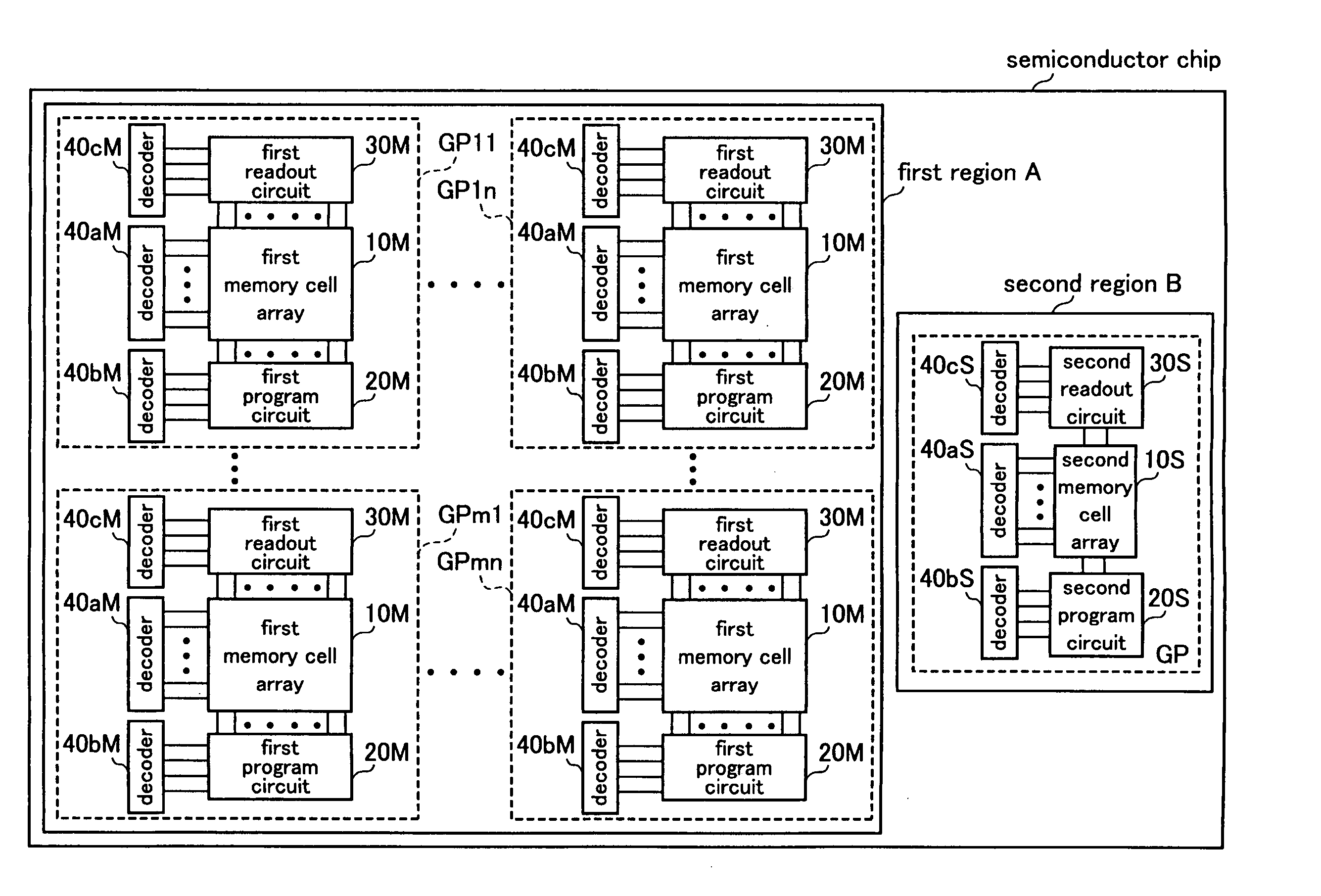
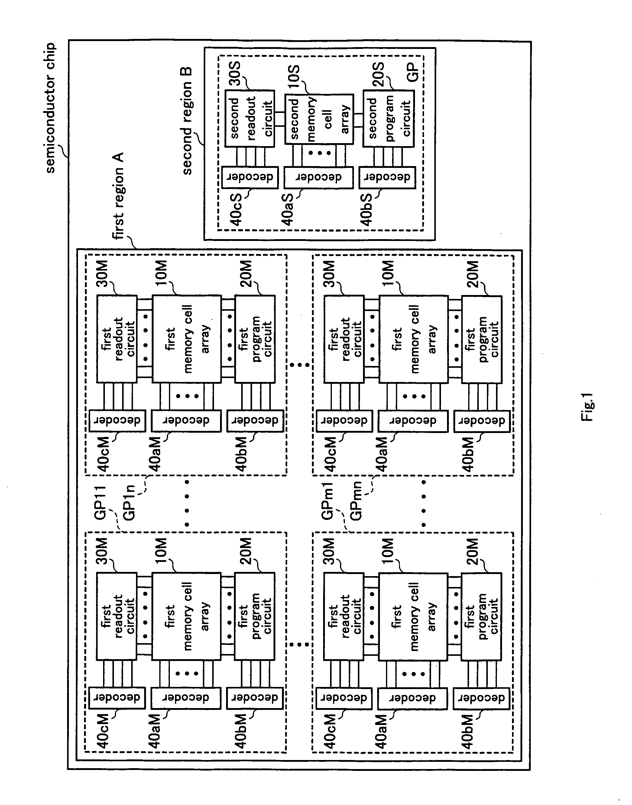
[0026]FIG. 1 is a schematic block diagram showing a semiconductor chip of a nonvolatile semiconductor memory according to a first embodiment of the present invention. General description will be given below of the nonvolatile semiconductor memory according to the first embodiment.
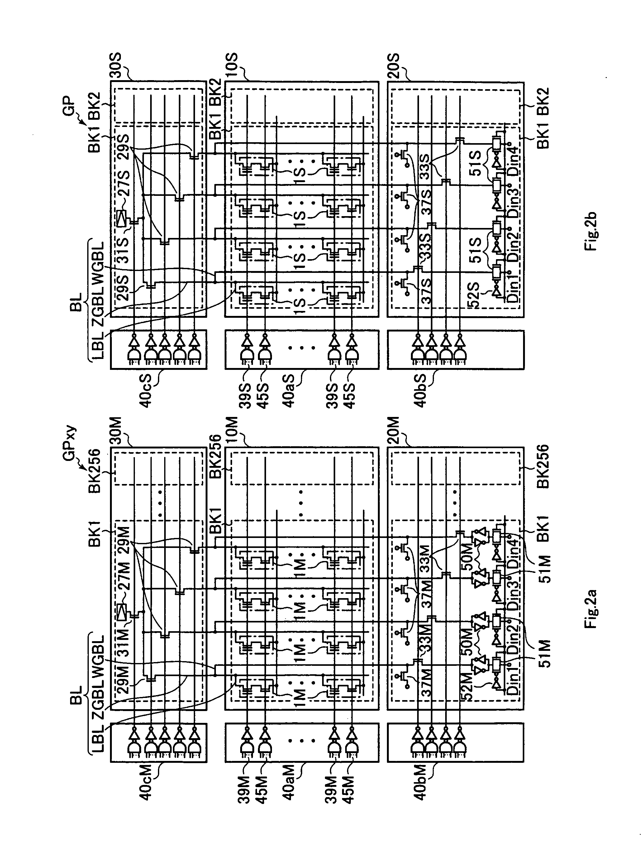
[0027] As shown in FIG. 1, the semiconductor chip of the nonvolatile semiconductor memory according to the first embodiment includes a first region A and a second region B. The first region A has a plurality of groups GPxy (x=1, 2, 3, . . . m, and y=1, 2, 3, . . . n), each group including a first memory cell array 10M, a first program circuit 20M, a first readout circuit 30M, and decoders 40aM, 40bM and 40cM.
[0028] The second region B has a group GP including a second memory cell array 10S, a second program circuit 20S, a second read circuit 30S, and decoders 40aS, 40bS and 40cS.
[0029] The first program circuit 20M and the first readout circuit 30M are used for write and read operations to memory cells a...
second embodiment
[0072] A second embodiment is an example where both of first and second memory cell arrays include one transistor type of the memory cells.
(1) First and Second Memory Cells and Peripheral Circuits Thereof
[0073]FIG. 6 shows a block diagram of one transistor type of a first memory cell and a peripheral circuit thereof according to the second embodiment of the present invention. FIG. 7 shows a block diagram of one transistor type of a second memory cell and a peripheral circuit thereof according to the second embodiment of the present invention. The first and second memory cells and the peripheral circuits thereof according to the second embodiment will be described below.
[0074] As shown in FIGS. 6 and 7, the second embodiment is different from the first embodiment in that the memory cells are a one-transistor type of memory cells and in that write inhibiting circuits and select gate decoders are not provided. To be more specific, the first and second memory cells 1M and 1S of the ...
third embodiment
[0078] A third embodiment is an example where first and second memory cells have different memory cell structures from each other.
[0079] Specifically, since the first memory cell 1M requires a fast writing speed to handle large volumes of data, a two-transistor type of the memory cell having a data writing speed faster than that of a one-transistor type of the memory cell is employed. Meanwhile, the second memory cell 1S does not require such a fast writing speed since the memory cell handles a small volume of data. Thus, as the second memory cell 1S, a one-transistor type of the memory cell capable of reducing a layout area, compared to the two-transistor type of the memory cell, is employed.
[0080] Here, the two-transistor type of the memory cell has the data writing speed faster than that of the one-transistor type of the memory cell because of the following reasons. In the one-transistor type of the memory cell, normally, a threshold distribution of “1” data and a threshold dis...
PUM
 Abstract
Description
Claims
Application Information
 - R&D
- Intellectual Property
- Life Sciences
- Materials
- Tech Scout
- Unparalleled Data Quality
- Higher Quality Content
- 60% Fewer Hallucinations
Browse by: Latest US Patents, China's latest patents, Technical Efficacy Thesaurus, Application Domain, Technology Topic, Popular Technical Reports.
© 2025 PatSnap. All rights reserved.Legal|Privacy policy|Modern Slavery Act Transparency Statement|Sitemap|About US| Contact US: help@patsnap.com