
Automated and customizable generation of efficient test programs for multiple electrical test equipment platforms

a test program and test platform technology, applied in the field of creating efficient testing procedures, can solve the problems of time-consuming thorough testing, prolonging the product development cycle, and introducing a faulty or inefficient device into the marketpla

Inactive Publication Date: 2005-12-08
INTEL CORP
View PDF8 Cites 43 Cited by
  • Summary
  • Abstract
  • Description
  • Claims
  • Application Information

AI Technical Summary

Problems solved by technology

This research and development phase testing must be thorough, or a manufacturer runs the risk of introducing a faulty or inefficient device into the marketplace.
Although testing is important, thorough testing is time consuming and prolongs the product development cycle.
It takes a long time to generate test protocols and to train technicians on how to program and implement those test protocols.
The programming process is complicated by the fact that for different test equipment and for different tests, different instructions may be required.
Of course, it is not surprising that the differences in tests, test equipment, and testing languages leads to testing errors, and potential product roll-out delays.
Due to the enormity of test variables, and the test equipment or test language dependence of these variables, programmers are more likely to err in programming test parameters.
The process is very time consuming and potentially fraught with error, if rushed.
As a result of this manual test programming and data entry, testing programs are inefficient and may even produce completely useless data in extreme examples.
Programmers and technicians are simply more likely to input incorrect data if that data is test-, test equipment-, or test language-dependent, which semiconductor testing data invariably is.
And not only has manual data entry plagued semiconductor testing at the front end, error correction thus far has only been achieved manually, at the back end.
In fact, despite the error-prone nature of data entry, no automated techniques for validating test programs exist.

Method used


Image

  • Automated and customizable generation of efficient test programs for multiple electrical test equipment platforms
  • Automated and customizable generation of efficient test programs for multiple electrical test equipment platforms
  • Automated and customizable generation of efficient test programs for multiple electrical test equipment platforms

Examples


Embodiment Construction

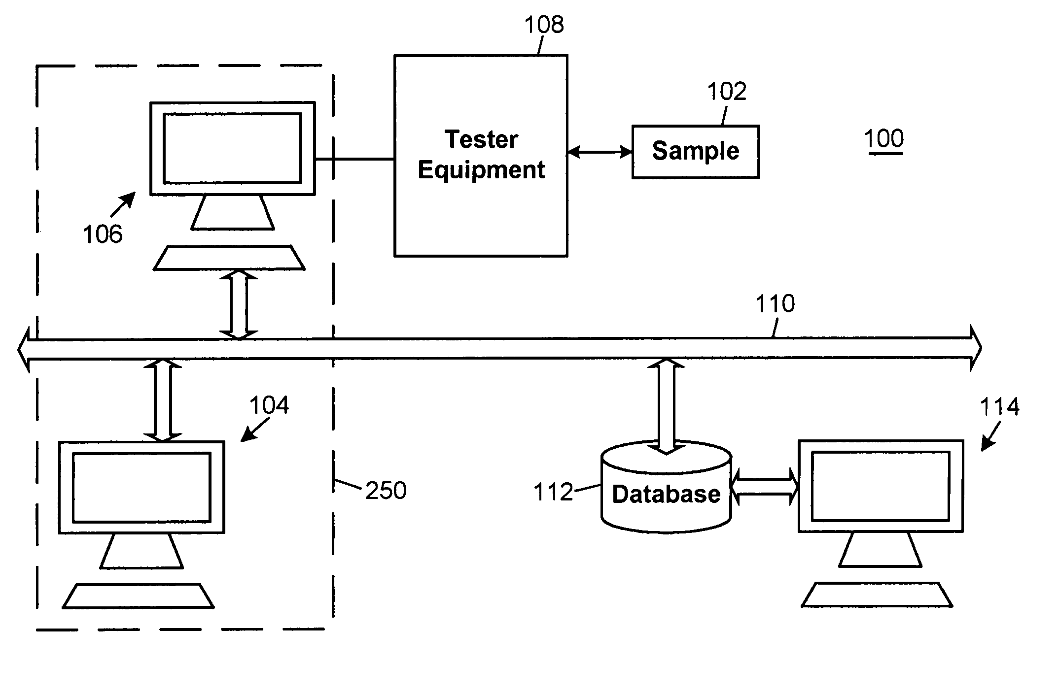
[0027] Numerous techniques are described for creating efficient semiconductor device test programs that may be used on multiple electrical tester equipment platforms. The techniques allow users to select various test algorithms, in the form of a number of test templates, to be run on a sample. Once a user selects a number of test algorithms, the techniques may automatically create an entire test package of these test algorithms, whether these algorithms are specific to one type of test language abstraction or another. With some of the disclosed techniques, the amount of time to create the test package may be greatly reduced. This is true whether a technique automatically populates all of the data for a test package or just a portion of the data. Errors in test package creation are also reduced.

[0028] Techniques are able to generate code for different tester equipment and test algorithms without having to change the test package format or definitions.

[0029] In some of the examples ...


PUM


Abstract

Automating techniques provide a way to create efficient test programs for characterizing semiconductor devices, such as those on a silicon die sample. Typically, test program creation is a drawn out process involving data entry for every test to be run as part of the test program. The described techniques improve test algorithm selection and automatically populate the test algorithm data in creating the test program. The automatic population may occur by accessing test structure, header, and test algorithm catalogs. The test structure catalog contains physical data for the test program, while the header catalog contains global parameter values. The test algorithm catalog has all of the various test algorithms that may be run in a given test, where these test algorithms may be in a template form and specific to any number of different test language abstractions. After test program creation, a validation process is executed to determine if the test program data is valid. Invalid data may be flagged, in an example. Once validated, techniques are described for converting the validated test program into an executable form, by formatting the various test algorithm data in the test program into a form compatible with the applicable test language abstraction selected by the user or the tester.

Description

FIELD OF THE INVENTION [0001] The present disclosure relates generally to semiconductor circuit testing and, more specifically, to creating efficient testing procedures that may be used by different testing equipment. BACKGROUND OF RELATED ART [0002] Microprocessor manufacturers are continually developing and testing new circuit designs, primarily to meet the market's desire for smaller, faster, and more powerful microprocessors. Yet, before creating a new microprocessor, manufacturers must first figure out ways of creating smaller transistors, capacitors, inductors, fuses, ring oscillators, etc., i.e., the constituent circuit elements that form today's microprocessors. As a result, manufacturers view semiconductor device testing as invaluable to all phases of product development, from research and development to final product validation. [0003] In the research and development phase, a manufacturer may spend months designing, building, and testing new layouts and manufacturing proce...

Claims


Application Information

Patent Timeline
IPC IPC(8): G01R31/28G06F11/00G06F11/263
CPCG06F11/263
Inventor SACHDEV, SANJAYWINSTEAD, CHARLES H.
Owner INTEL CORP
Learn More