Chip-component-mounted device and semiconductor device

a semiconductor device and component technology, applied in the direction of printed circuit non-printed electric components association, sustainable manufacturing/processing, final product manufacturing, etc., to achieve the effect of stabilizing connection strength and increasing connection strength

a semiconductor device and component technology, applied in the direction of printed circuit non-printed electric components association, sustainable manufacturing/processing, final product manufacturing, etc., to achieve the effect of stabilizing connection strength and increasing connection strength

US20050275090A1Inactive Publication Date: 2005-12-15NEC ELECTRONICS CORP

Image

  • Chip-component-mounted device and semiconductor device
  • Chip-component-mounted device and semiconductor device
  • Chip-component-mounted device and semiconductor device

Examples


Embodiment Construction

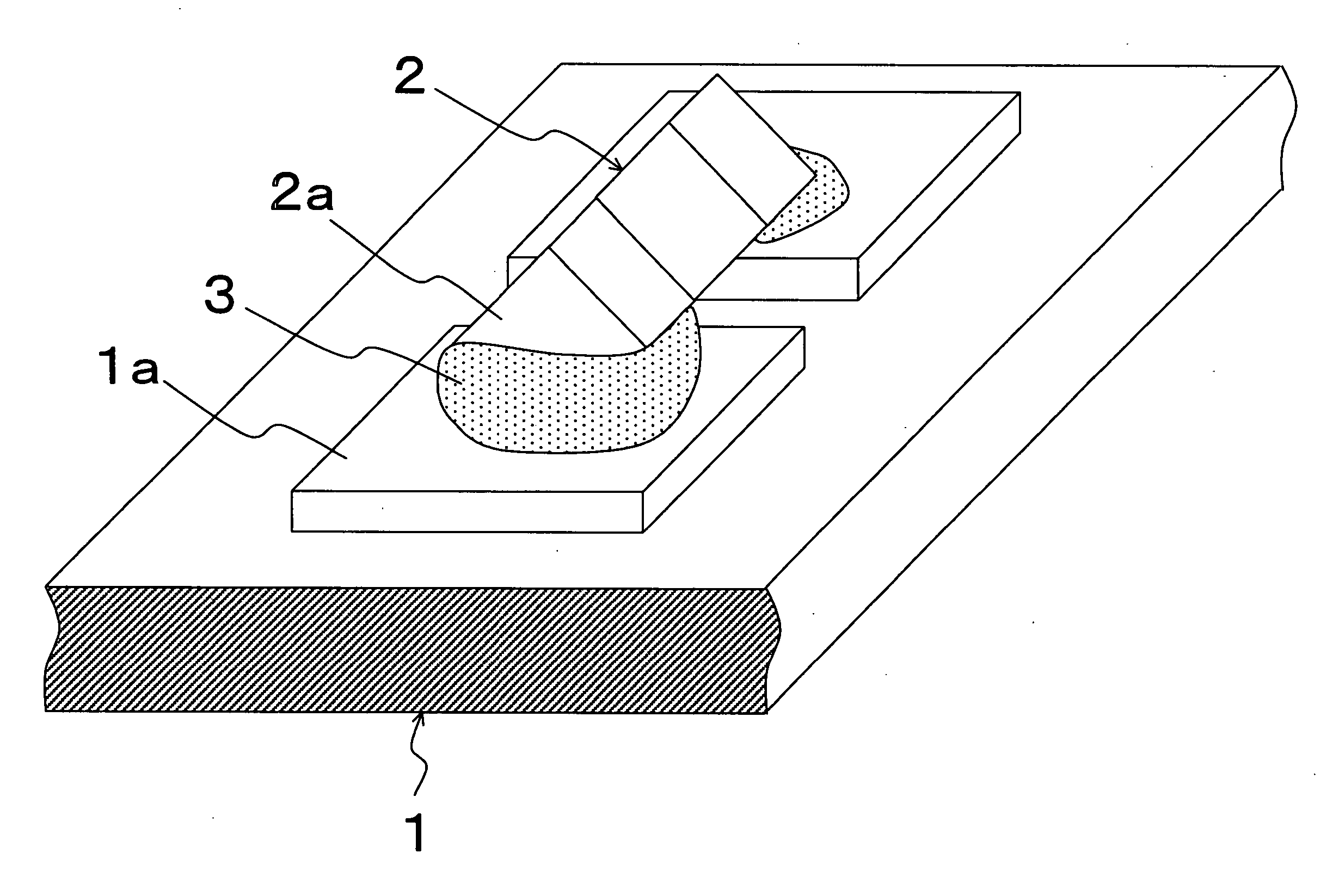
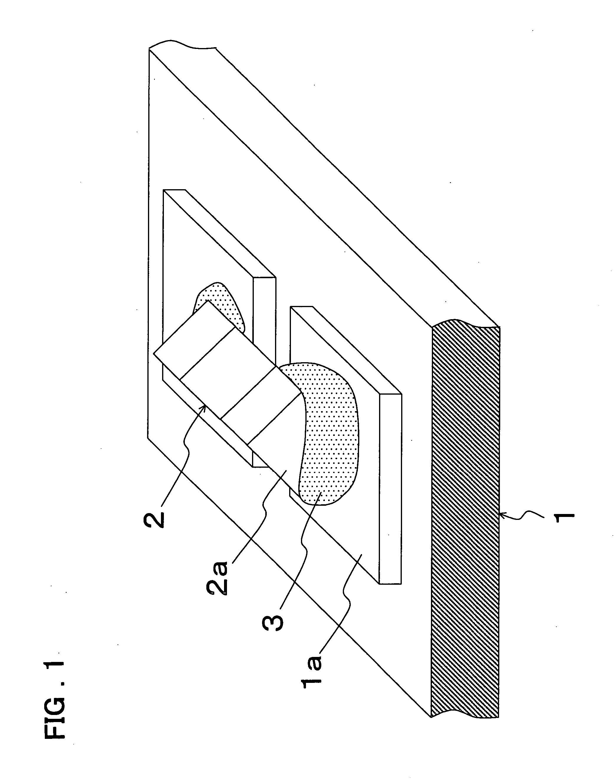
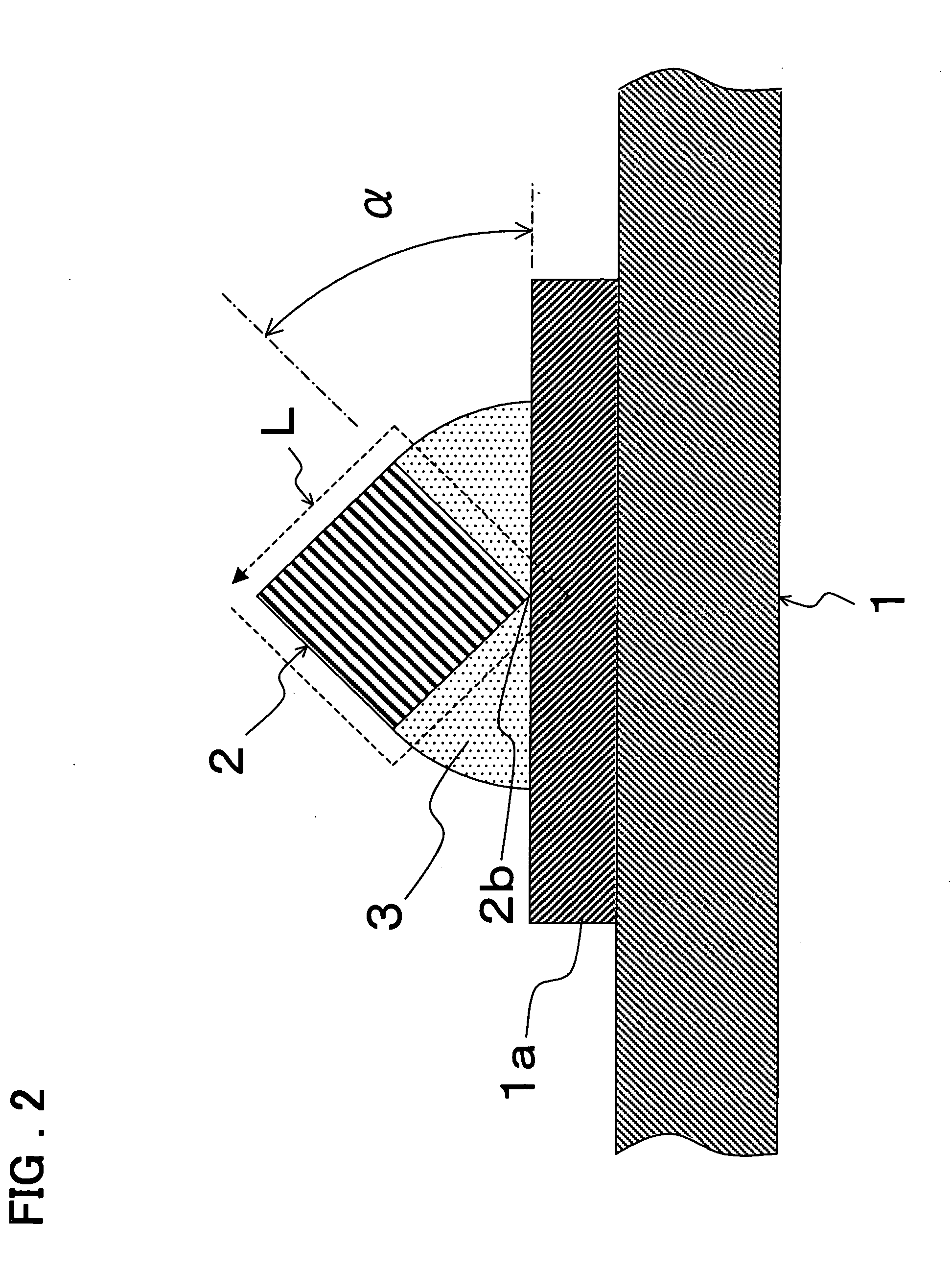
[0027] A chip-component-mounted device according to a first embodiment of the present invention is explained below with reference to drawings. FIG. 1 is a partially perspective view schematically showing a structure of the chip-component-mounted device according to the first embodiment of the present invention. FIG. 2 is a partially cross-sectional view schematically showing a structure of the chip-component-mounted device according to the first embodiment of the present invention.

[0028] In the first embodiment, a chip component 2 is arranged on two pads 1a (connected parts) of a print wiring board 1, on which a semiconductor element (not shown) is mounted, so as to bridge between two pads 1a, a corner part 2b of the chip component 2 facing toward the pad 1a side. The pad 1a and an electrode part 2a corresponding to the pad 1a are connected each other through an electrically conductive adhesive 3 physically and electrically. The pad 1a of the print wiring board 1 is an electrically...


PUM


Abstract

A chip-component-mounted device comprises a print wiring board or lead frame, an electrically conductive adhesive and a chip component, said chip component being mounted on said print wiring board or lead frame through said electrically conductive adhesive, said chip component having a corner part, a ridgeline of said corner part facing a connected part side of said print wiring board or lead frame, an angle made by a face adjacent to said ridgeline and a face of said connected part being acute.

Description

FIELD OF THE INVENTION [0001] The present invention relates to a chip-component-mounted device and semiconductor device in which a chip component is mounted on a print wiring board or lead frame, and, particularly, to a chip-component-mounted device and semiconductor device which can prevent a short circuit with an adjacent pad (or lead) and component. BACKGROUND OF THE INVENTION [0002] In recent years, a semiconductor device in which a semiconductor element is mounted on a print wiring board (or lead frame) is becoming higher in density, and there is an increasing importance of a semiconductor device of a module type, in which a chip component is mounted. The chip component, such as a bypass condenser for stabilization of power source, a condenser for stabilization of circuit operation, a load resistance, an inductance or the like, is disposed around the semiconductor element. In most of the semiconductor devices of the module type, the semiconductor element and chip component are ...

Claims


Application Information

Patent Timeline
15 Dec 2005
Publication
US20050275090A1
IPC
H05K1/02; H05K1/11; H05K3/32; H05K1/18; H01L21/60; H01L23/48
CPC
H05K1/111; H05K3/321; H05K2201/09745; H05K2201/10484; H05K2201/10636; H01L2924/0002; H01L2924/00; Y02P70/611
Inventors
NAKAZAWA, TAIBO