System and method for the probing of a wafer

a technology of probing system and wafer, which is applied in the field of electronic component testing, can solve the problems of reducing the integrity of the wafer, reducing the accuracy of the results, and requiring several hours of single probing session testing, so as to reduce the disadvantages and problems associated with single probing session.

Active Publication Date: 2005-12-15
TEXAS INSTR INC
View PDF13 Cites 7 Cited by
  • Summary
  • Abstract
  • Description
  • Claims
  • Application Information

AI Technical Summary

Benefits of technology

[0004] From the foregoing it may be appreciated by those skilled in the art that a need has arisen for a system and method for the probing of a wafer. In accordance with the present invention, a system and method for the probing of a wafer is provided that substantially eliminates or greatly reduces disadvantages and problems associated with conventional wafer testing equipment.
[0006] Depending on the specific features implemented, particular embodiments of the present invention may exhibit some, none or all of the following technical advantages. Various embodiments may be capable of resuming a probing session of a wafer even after a prior probing session is aborted. The resumed probing session may utilize data that was gathered in the earlier aborted probing session. Accordingly, some embodiments may be capable of storing the data gathered about each die during the earlier probing session and using the stored data to determine the one or more die on the wafer that remain untested. As a result, only the untested die may be probed during the resumed probing session.
[0008] Other embodiments may be capable of easily and quickly generating a probe map of the wafer since the data generated from any previously aborted probing sessions may be stored in a relational database. After multiple partial probing sessions are performed and the probing of the wafer is complete, the data gathered from each probing session may be merged for reporting purposes. Accordingly, problems associated with previous methods and systems for resumed probing of a wafer may be reduced, and the quality and functionality of the integrated circuit or other components supported on the wafer may be improved.

Problems solved by technology

For example, a single probing session may require several hours of testing time.
Regardless of the cause, when a probing session is aborted, the time spent performing the probing session and the data gathered from the probing session are typically lost.
Because each probing session of a wafer results in wear to each die tested on the wafer, multiple probing sessions performed on a wafer may degrade the integrity of the wafer.

Method used


Image

  • System and method for the probing of a wafer
  • System and method for the probing of a wafer
  • System and method for the probing of a wafer

Examples


Embodiment Construction

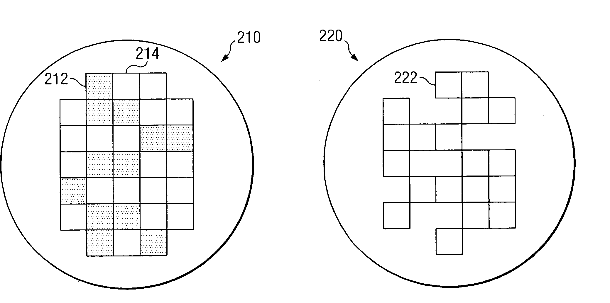
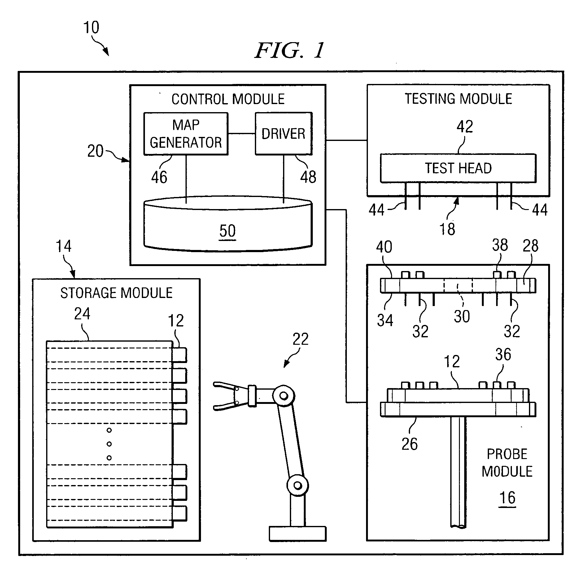
[0015]FIG. 1 is a block diagram of a system 10 for the probing of a wafer 12 after one or more partial probing sessions have been aborted. In various embodiments, wafer 12 may include a thin polished slice of crystal material sliced from a crystal cylinder grown for the purpose of semiconductor fabrication. According to one typical fabrication technology, a wafer may be eight inches in diameter and provide the foundation on which a semiconductor device may be created. The semiconductor device may be created on the surface of the wafer using a variety of techniques and procedures, such as layering, photolithographic patterning, doping through implantation of ionic impurities, and heating. The starting material may comprise silicon, gallium arsenide, or other suitable substrate material. As will be described in further detail below, system 10 includes a storage module 14, a probe module 16, a testing module 18, and a control module 20 and may include any other modules appropriate for ...


PUM


Abstract

According to one embodiment of the invention, a method for resuming the probing of a wafer includes identifying a data set associated with a wafer. The data set identifies at least one unprobed die supported on the surface of the wafer. The method also includes determining that the data set associated with the wafer is useable and generating a probe map of the wafer from the data set. The probe map identifies a physical position associated with each unprobed die supported on the surface of the wafer. The probe map and one or more probe commands are communicated to a probe module to drive the probe module in resuming the probe of the wafer.

Description

TECHNICAL FIELD OF THE INVENTION [0001] This invention relates in general to the testing of electronic components, and more particularly to a system and method for the probing of a wafer. BACKGROUND OF THE INVENTION [0002] An array of die, which may include integrated circuits and their components, are typically supported on a wafer during various semiconductor fabrication processes. At various stages during fabrication processes, it may be desirable to perform testing on each die to read information from each die, write information to each die, or otherwise gather information about each die and components on each die. During testing, a probe map is downloaded to a prober and is then used by the prober to position the wafer to sequentially align each die on the wafer with testing equipment. [0003] Although it is generally desirable to test each die on the wafer in a single pass, or probing session, in certain situations the probing session may be aborted before every die on the wafe...

Claims


Application Information

Patent Timeline
Patent Type & Authority Applications(United States)
IPC IPC(8): G01R31/26G01R31/28
CPCG01R31/2834G01R31/2894
Inventor SCHUETTE, GLENN E.ROUSEY, JAMES E.MILLER, CURTIS E.
Owner TEXAS INSTR INC
Why Eureka
Try Eureka