System and method for improved dopant profiles in CMOS transistors

a technology of cmos transistor and dopant profile, which is applied in the field of system and method for improving the dopant profile of cmos transistor, can solve the problems of reducing the scale of semiconductor devices, reducing the reliability of the gate stack as a conductor, and reducing the difficulty of diffusion of dopants through the gate stack, etc., and achieves the effect of reducing disadvantages or greatly reducing problems

Active Publication Date: 2006-05-11
TEXAS INSTR INC
View PDF5 Cites 5 Cited by
  • Summary
  • Abstract
  • Description
  • Claims
  • Application Information

AI Technical Summary

Benefits of technology

[0003] In accordance with the present invention, a system and method for forming semiconductor devices on the surface of the wafer is provided that substantially eliminates or greatly reduces disadvantages and problems associated with conventional semiconductor fabrication equipment.

Problems solved by technology

As semiconductor manufacturers continue to reduce the scale of semiconductor devices, however, the diffusion of dopants through the gate stack becomes more difficult.
Where the concentration of dopant at the desired interface is too low, the reliability of the gate stack as a conductor may be reduced and the ability of the gate stack to control the conductivity of the channel can be impeded.

Method used


Image

  • System and method for improved dopant profiles in CMOS transistors
  • System and method for improved dopant profiles in CMOS transistors
  • System and method for improved dopant profiles in CMOS transistors

Examples


Embodiment Construction

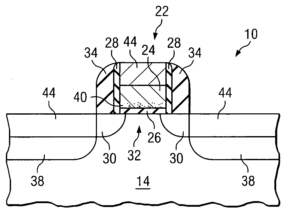
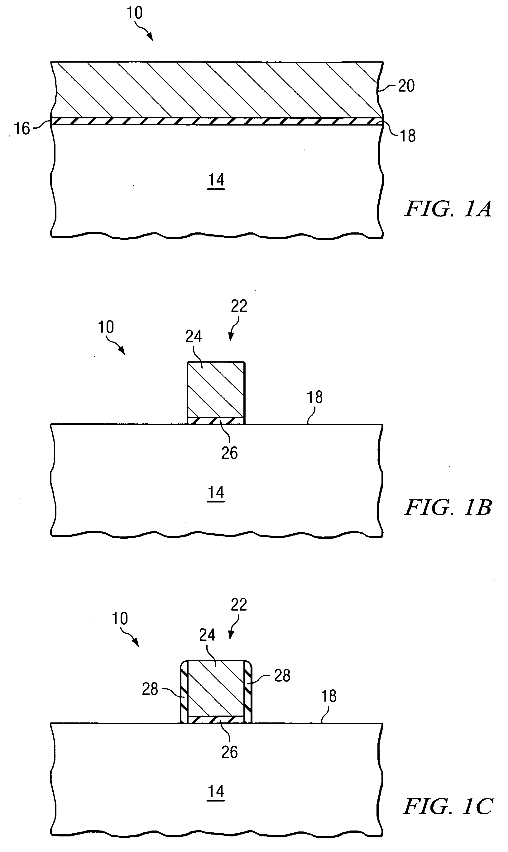
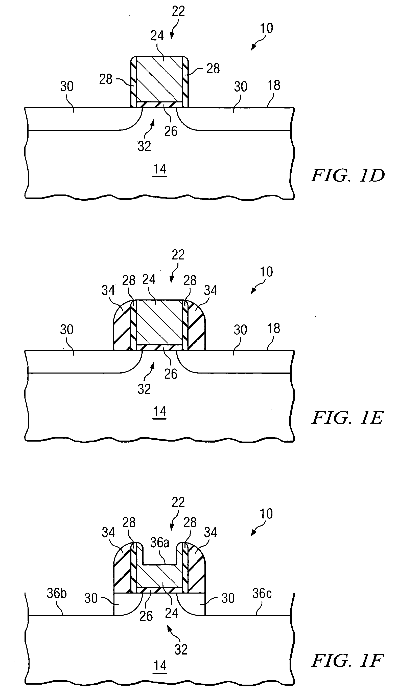
[0010] In order to form an integrated circuit device such as a field effect transistor, various conductive and nonconductive layers are typically deposited or grown on a semiconductor body or other outer semiconductor layer. FIGS. 1A-1H are cross-sectional views of a semiconductor structure 10 during the formation of multiple layers on an outer surface of a semiconductor body 14. Semiconductor structure 10 may be used as a basis for forming any of a variety of semiconductor devices, such as a bipolar junction transistor, an NMOS transistor, a PMOS transistor, a CMOS transistor, a diode, a capacitor, or other semiconductor based device. Particular examples and dimensions specified through out this document are intended for exemplary purposes only, and are not intended to limit the scope of the present disclosure. Moreover, the illustration in FIGS. 1A-1G are not intended to be to scale. As will be discussed in more detail below, conventional semiconductor fabrication techniques for f...


PUM


Abstract

According to one embodiment of the present invention, a method of forming a semiconductor device includes forming a gate stack on an outer surface of a semiconductor body. First and second sidewall bodies are formed on opposing sides of the gate stack. A first recess is formed in an outer surface of the gate stack, and a first dopant is implanted into the gate stack after the first recess is formed. The first dopant diffuses inwardly from the outer surface of the gate stack that defines the first recess. The first dopant diffuses toward an interface between the gate stack and the semiconductor body. The first recess increases the concentration of the first dopant at the interface.

Description

FIELD OF INVENTION [0001] The present invention relates generally to semiconductor devices and more particularly to a system and method for improved dopant profiles in CMOS transistors. BACKGROUND OF THE INVENTION [0002] During the fabrication of certain types of semiconductor devices, a gate stack may be formed on the surface of a semiconductor body. The area of the semiconductor body that lies below the gate stack defines a selectively conductive channel region. Various conductive regions in the semiconductor device may be formed by the implantation of one or more dopants into the layers of the semiconductor device. For example, a dopant may be implanted within the semiconductor body on either side of the gate stack to form source and drain regions. Additionally, a dopant may be implanted into and diffused through the gate stack to improve the conductivity of the gate stack. Specifically, the dopant migrates through the gate stack in a substantially vertical direction toward an in...

Claims


Application Information

Patent Timeline
Patent Type & Authority Applications(United States)
IPC IPC(8): H01L21/8232H01L21/8234
CPCH01L21/28044H01L21/28176H01L21/823842H01L29/4925H01L29/66545H01L29/6656H01L29/6659H01L29/66636H01L29/7833
Inventor CHIDAMBARAM, PRCHAKRAVARTHI, SRINIVASAN
Owner TEXAS INSTR INC
Why Eureka
Try Eureka