Chip resistor and method for manufacturing the same

a technology of resistors and chips, applied in the field of chip resistors, can solve the problems of fluctuation of resistance value of resistor films, excessive total positioning error, and easy fluctuation of resistan

Active Publication Date: 2005-12-15
ROHM CO LTD
View PDF4 Cites 10 Cited by
  • Summary
  • Abstract
  • Description
  • Claims
  • Application Information

AI Technical Summary

Benefits of technology

[0014] It is an object of the present invention to provide a technique of eliminating the foregoing p

Problems solved by technology

Generally, chip resistors constituted of a chip-type insulating substrate and a resistant film provided on the upper surface thereof are not provided with sufficient surge resistance, and hence the resistance is prone to fluctuate when a surge voltage is applied, for example because of an influence of static electricity or a power source noise.
This results in fluctuation in resistance value of the resistant film.
However, since a positional shift incurred in the screen p

Method used


Image

  • Chip resistor and method for manufacturing the same
  • Chip resistor and method for manufacturing the same
  • Chip resistor and method for manufacturing the same

Examples


first embodiment

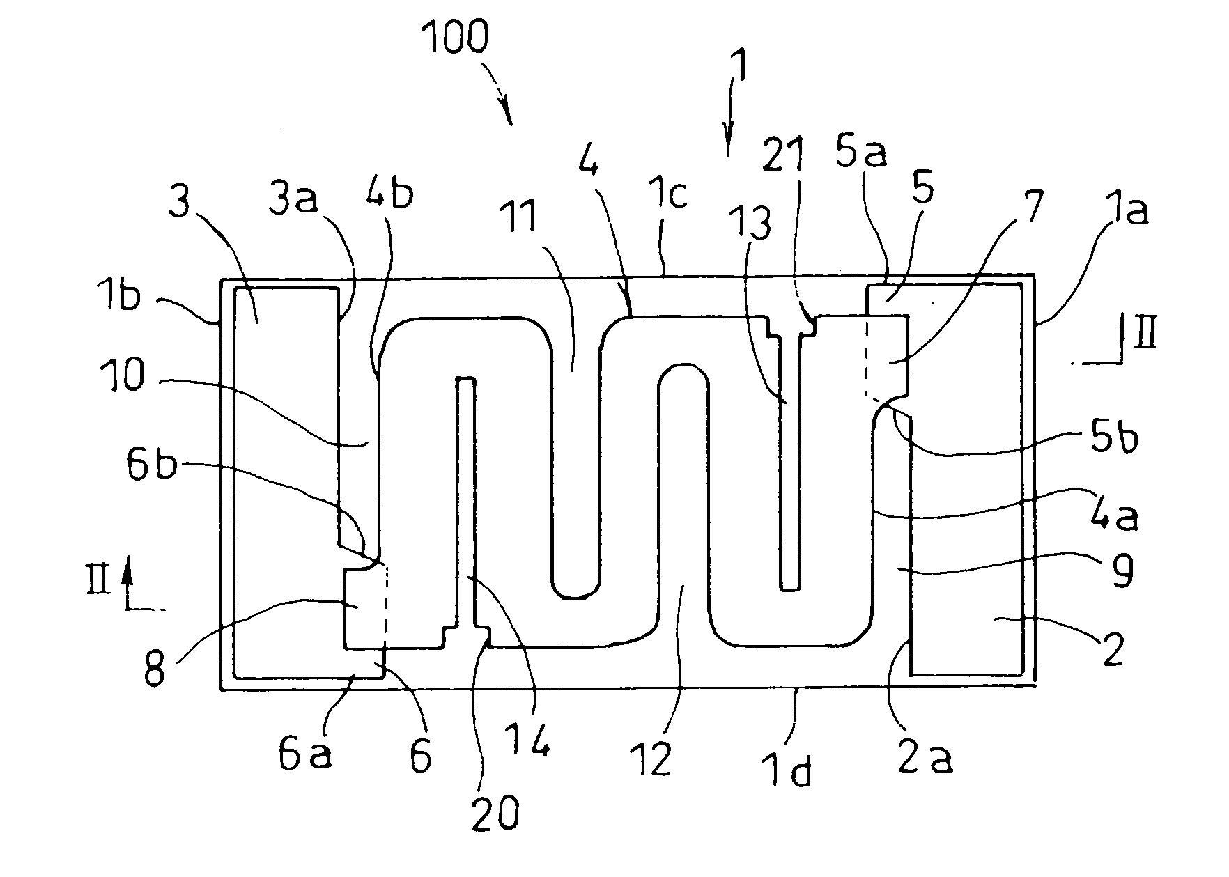
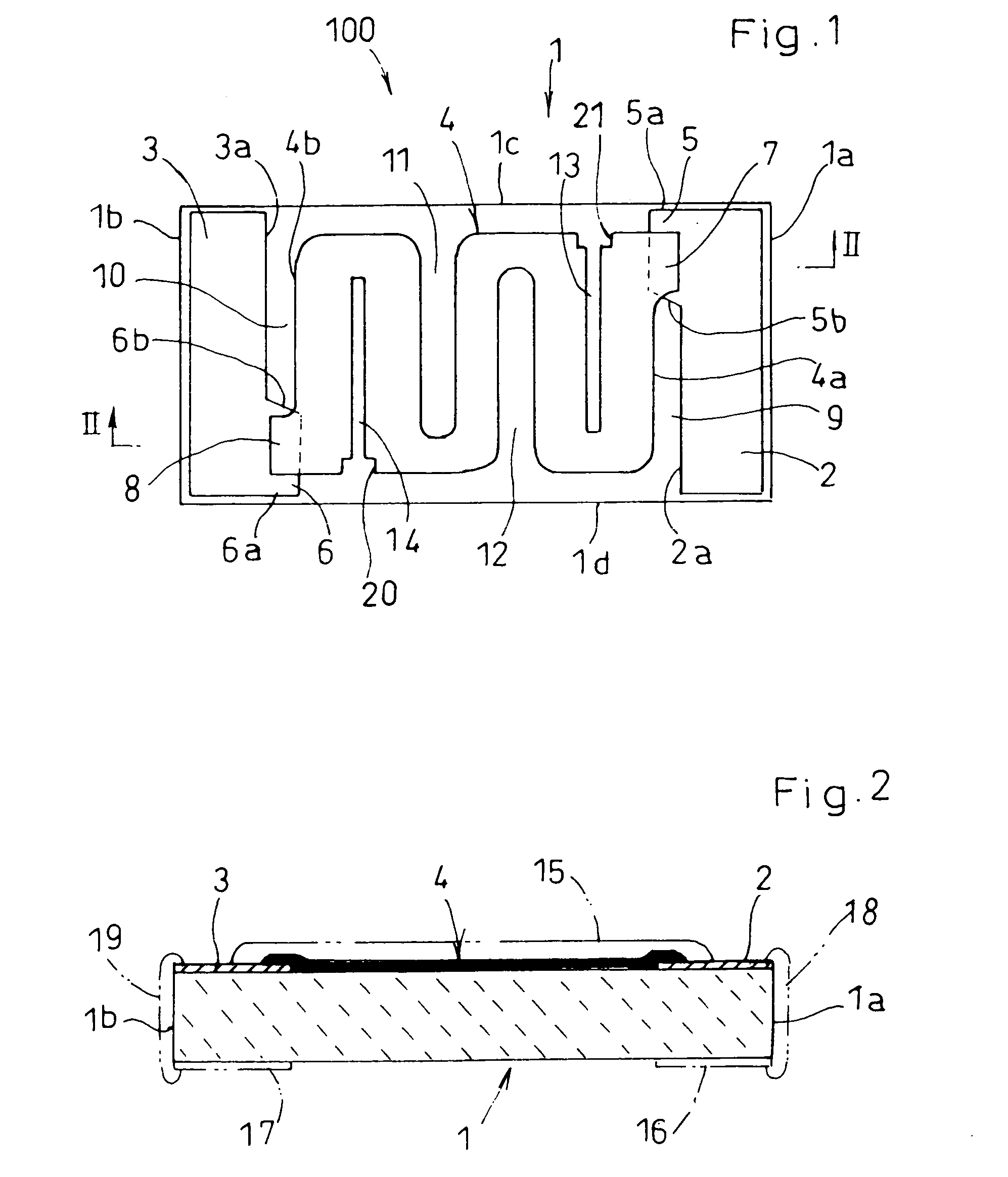
[0036] FIGS. 1 to 3 depict a chip resistor according to the present invention.

[0037] The chip resistor 100 includes a chip substrate 1 made of a heat-resistant insulating material such as a ceramic and formed in a rectangular shape, and a terminal electrode 2, 3 located on the upper surface of the chip substrate 1 in a region close to the respective ends 1a, 1b in a longitudinal direction, by screen-printing the paste of the terminal electrode material and a subsequent sintering process.

[0038] In a region between the terminal electrodes 2, 3 on the upper surface of the chip substrate 1, a resistant film 4 of an appropriate width (width W0) is provided so as to extend in a longitudinal direction of the chip substrate 1, by screen-printing the paste of the resistant film material and a subsequent sintering process.

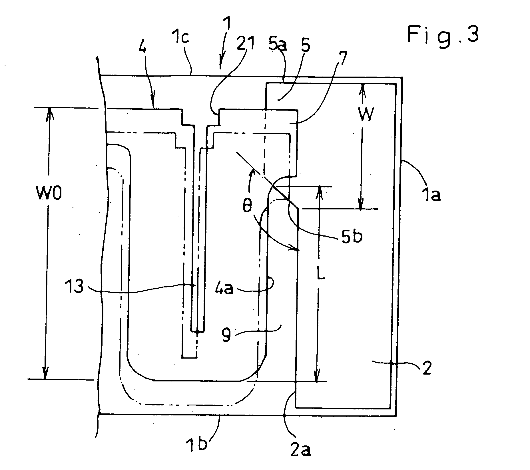
[0039] When forming the terminal electrodes 2, 3, the inner edge 2a of the terminal electrode 2a includes a protrusion 5 located in a portion close to a side edge 1c of th...

second embodiment

[0049] When performing the processing work of engraving the second slits 13, 14 on the resistant film 4, a cutaway portion 20, 21 is provided at the respective positions on the resistant film 4 where the processing work for forming the second slits 13, 14 is supposed to be started, simultaneously with the formation of the resistant film 4 by screen printing or the like. The cutaway portions 20, 21 serve to facilitate identifying the position to start the processing work of engraving the second slits 13, 14, with high precision. Details of this effect will be described based on a

[0050] The second embodiment of the present invention will now be described referring to FIGS. 4 to 7, among which FIGS. 4 and 5 depict a chip resistor 100′ according to the second embodiment.

[0051] The chip resistor 100′ includes a chip substrate 101 made of a heat-resistant insulating material such as a ceramic and formed in a rectangular shape having a width D0 and a length L0, a terminal electrode 102, 1...


PUM


Abstract

A chip resistor includes a chip substrate, a terminal electrode formed on an upper surface of the chip substrate in a region close to the respective end portions, and a resistant film formed in a zigzag-folded shape on the upper surface of the chip substrate between the terminal electrodes. An inner edge of at least one of the terminal electrodes includes a protrusion integrally formed so as to project from a portion close to a side edge of the chip substrate toward the resistant film, for achieving electrical connection between the resistant film and the protrusion. A side edge of the protrusion facing inward farther from the side edge of the chip substrate is inclined such that a front edge of the protrusion has a narrower width.

Description

TECHNICAL FIELD [0001] The present invention relates to a chip resistor including a chip-type insulating substrate and a resistant film provided on the upper surface of the substrate, particularly to a chip resistor having an upgraded surge resistance, and to a method for manufacturing the same. BACKGROUND ART [0002] Generally, chip resistors constituted of a chip-type insulating substrate and a resistant film provided on the upper surface thereof are not provided with sufficient surge resistance, and hence the resistance is prone to fluctuate when a surge voltage is applied, for example because of an influence of static electricity or a power source noise. For improving the surge resistance, extending a length of a path on the resistant film through which a current runs is known as an effective remedy. [0003] Accordingly, a conventional chip resistor is provided with a terminal electrode on the respective longitudinal end portions on the upper surface of the substrate made of a hea...

Claims


Application Information

Patent Timeline
IPC IPC(8): H01C17/00H01C1/14H01C1/012H01C7/00H01C17/28
CPCH01C1/14H01C7/003H01C3/12H01C17/281H01C17/006
Inventor YONEDA, MASAKI
Owner ROHM CO LTD
Why Eureka
Try Eureka