Display apparatus

Active Publication Date: 2005-12-15
SHARP KK
View PDF8 Cites 19 Cited by
  • Summary
  • Abstract
  • Description
  • Claims
  • Application Information

AI Technical Summary

Benefits of technology

[0025] The second display apparatus is a display apparatus that carries out the time-division gradation driving in accordance with turning ON/OFF of the second transistor, and is so set that a current constantly flows through the first transistor while the third transistor is OFF. This appropriately secures not only time required for the setting of the output current of the driving transistor for attainment of the time-division gradation display, but also the required number of pixels for the display.
[0026] As described above, each of the first display apparatus and the second display appar

Problems solved by technology

Conventional passive matrix driving suffers from a difficulty in attainment of high luminance due to an increase in the number of scan lines, and from a decrease in duration due to momentary application of a very large current to pixels.
Incidentally, big problems of the active matrix driving are (i) current non-uniformity due to property variation of a thin film transistor (TFT), and (ii) uneven display luminance due to threshold voltage non-uniformity thereof.
Other problems are (i) a decrease in luminance due to a deterioration of the organic EL with age, and (ii) a change (as temperature rises, the luminance rises) in luminance due to light emission (heat emission) of the organic EL.
However, the driving method in Document 1 requires 60 microseconds

Method used


Image

  • Display apparatus
  • Display apparatus
  • Display apparatus

Examples


embodiment 1

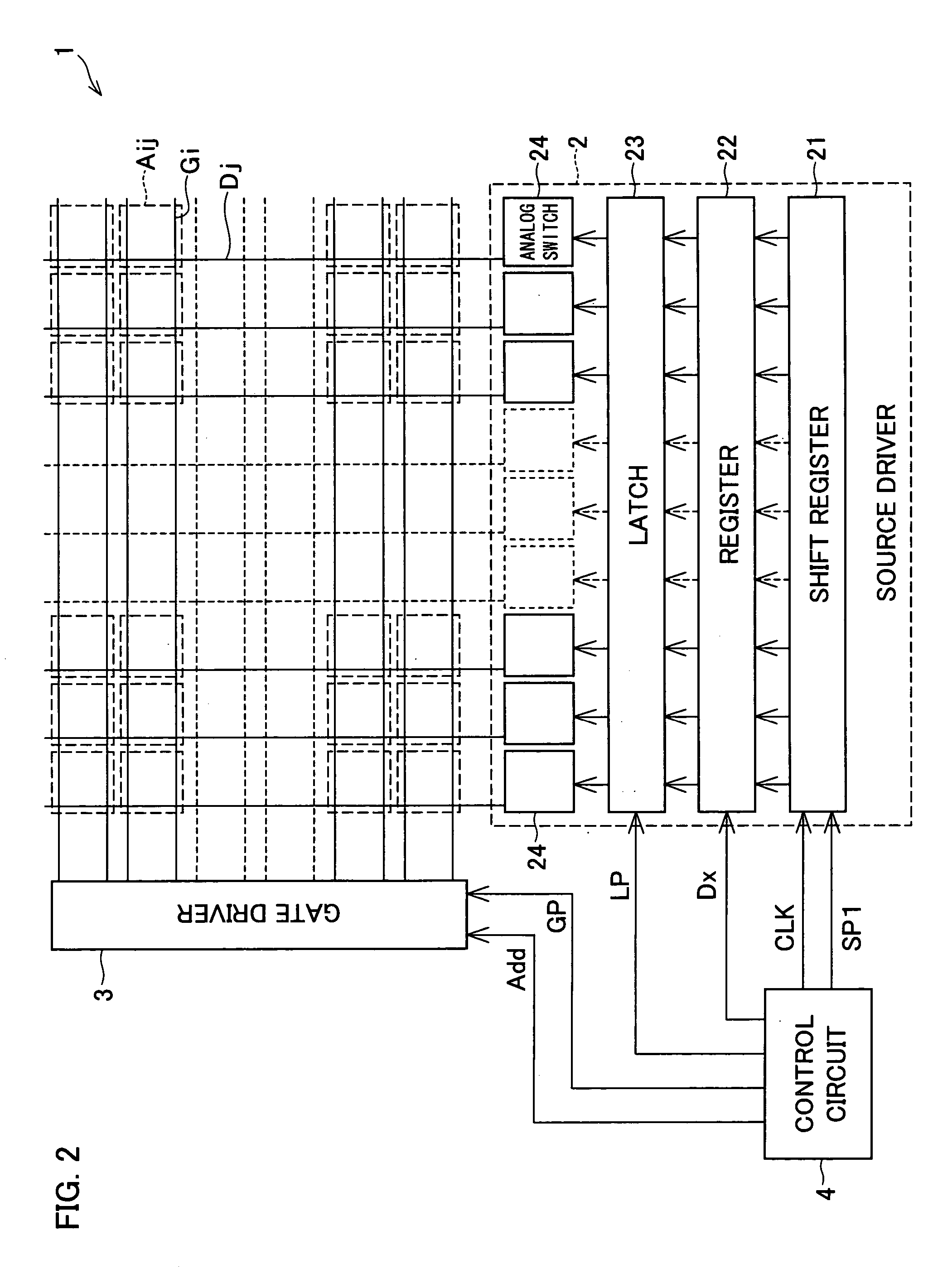
[0063] Firstly, Embodiment 1 is explained. FIG. 2 is a block diagram illustrating an entire circuit structure of an organic EL display apparatus 1 of the present embodiment.

[0064] As shown in FIG. 2, the organic EL display apparatus 1 includes (i) a plurality of pixel circuits Aij (i=1 through m; j=1 through n), (ii) a source driver 2, and (iii) a gate driver 3.

[0065] Provided in the organic EL display apparatus 1 are (i) a plurality of data wires Dj (data lines) parallel to each other; and (ii) a plurality of scan wires Gi that are parallel to each other and that are perpendicular to the data wires Dj, respectively. In respective intersections of the data wires Dj and the scan wires Gj, the pixel circuits Aij (pixels) are provided in a matrix manner. The gate wires Dj are connected to a source driver 2, whereas the scan wires Gi are connected to a gate driver 3.

[0066] For size reduction of the entire display apparatus and manufacture cost reduction thereof, it is preferable that...

embodiment 2

[0106] Next, Embodiment 2 is explained. FIG. 6 is a block diagram illustrating an entire circuit structure of an organic EL display apparatus 11 of the present embodiment.

[0107] As is the case with the foregoing organic EL display apparatus 1, the organic EL display apparatus 11 includes (i) a plurality of pixel circuits Aij (i=1 through m; j=1 through n), (ii) a source driver 2, and (iii) a gate driver 3 as shown in FIG. 6. However, the original EL display apparatus 11 further includes a current driver 5 and a reference current source 6.

[0108] The current driver 5 includes a shift register 51 and a plurality of current driving circuits 52.

[0109] The shift register 51 receives a start pulse SP2 from a control circuit 4, and transfers the start pulse SP1 in synchronization with a clock SLK, and outputs the start pulse SP2, as a timing signal, from respective output stages. The clock SLK has a frequency f(SLK) that is different from a frequency f(CLK) of the aforementioned clock CL...

embodiment 3

[0136] Next, Embodiment 3 is explained.

[0137] As is the case with Embodiment 2, an organic EL display apparatus 11 of the present embodiment includes a plurality of pixel circuits Aij (i=1 through m; j=1 through n), a source driver 2, a gate driver 3, a current driver 5, and a reference current source 6, as shown in FIG. 6.

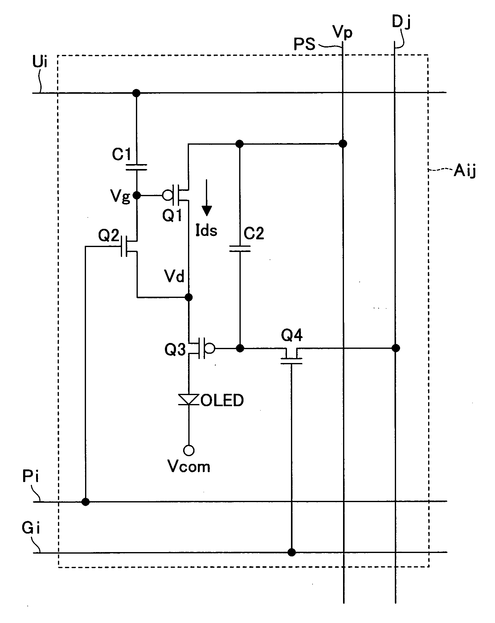
[0138]FIG. 11 is a circuit diagram illustrating a structure of each of the pixel circuits Aij of the present invention.

[0139] As shown in FIG. 11, the pixel circuit Aij includes an organic EL element OLED, transistors Q21 through Q26, and capacitors C21 through C23. Each of the transistors Q21 through Q26 is a TFT made of polycrystalline silicon or CG silicon. The transistor Q21 (first transistor) and the transistor Q25 (second transistor) are driving transistors. The pixel circuit Aij has such a circuit structure that the transistor Q21, the transistor Q25, and the organic EL element OLED (display element) are provided in series between (i) a power supply wire...


PUM


Abstract

When the transistor Q3 is OFF, a predetermined potential is supplied to a potential wire Ui such that a switching transistor Q2 becomes ON. This changes a gate potential of a driving transistor Q1 from an ON potential to a threshold potential. Thereafter, the transistor Q2 is turned OFF, with the result that the potential of the potential wire Ui is changed (in cases where the transistor Q1 is a p-type transistor, the potential is decreased). With this, the transistor Q1 allows a current to constantly flows therethrough, irrespective of the threshold potential. This shortens time for setting an output current of the driving TFT for driving a current driving type display element.

Description

[0001] This Nonprovisional application claims priority under 35 U.S.C. § 119(a) on Patent Application No. 2004 / 175867 filed in Japan on Jun. 14, 2004, and on Patent Application No. 2004 / 368434 filed in Japan on Dec. 20, 2004, the entire contents of which are hereby incorporated by reference. FIELD OF THE INVENTION [0002] The present invention relates to a display apparatus including a driving circuit for driving a current driving type display element such as an organic EL (Electro Luminescence) and an FED (Field Emission Display). BACKGROUND OF THE INVENTION [0003] An organic EL element serving as a current driving type display element has such a well-known property that luminance depends on a current value, and that duration is short when the organic EL element is driven by a large current for attainment of a high luminance display. Developed for acquirement of a wider display screen and high definition in a display apparatus including such an organic EL element is an active matrix...

Claims


Application Information

Patent Timeline
IPC IPC(8): G09G3/20G09G3/30G09G3/32
CPCG09G3/2022G09G3/325G09G3/3283G09G2300/0408G09G2320/043G09G2300/0809G09G2300/0852G09G2300/0861G09G2300/0417
Inventor NUMAO, TAKAJI
Owner SHARP KK
Why Eureka
Try Eureka