Operating techniques for reducing effects of coupling between storage elements of a non-volatile memory operated in multiple data states

a non-volatile memory and state operation technology, applied in the field of non-volatile memory, can solve the problems of significant adverse impact on the performance of the memory system, errors in reading the state of the first group,

Inactive Publication Date: 2005-12-15
TOSHIBA MEMORY CORP +1
View PDF26 Cites 44 Cited by
  • Summary
  • Abstract
  • Description
  • Claims
  • Application Information

AI Technical Summary

Benefits of technology

[0009] Therefore, according to one primary aspect of the present invention, a first group of memory storage elements are reprogrammed to their desired states after a second adjacent group of storage elements has been programmed. Since periodically reading the state of the cells is part of the programming process in order to know when to stop, the reprogramming places any additional charge on the first group of storage elements that is necessary to compensate for the effect of the field coupling with the later programmed adjacent storage elements. An alternating pulse and reading sequence of a typical programming operation may be used to reprogram the first group of storage elements in the presence of the effect of the second adjacent programmed group of storage elements. A later reading of the first group of cells, even though still influenced by the charge on adjacent cells, is now more accurate since the effect of the charge on the adjacent cells has been taken into account as a result of the reprogramming. In order to avoid having to maintain a data buffer that is large enough to hold the data programmed in the first pass for later use in the second programming pass, the data stored by the first pass may be read from the memory with adjusted read margins and then that data is reprogrammed in the second pass.
[0010] According to another primary aspect of the present invention, a distribution of programming levels among storage elements programmed to the same state is compacted by reprogramming some of the storage elements on one side of the distribution into the other side of the distribution. The storage elements of a given state are all read and those having programmed levels below a defined threshold within the distribution are given additional programming to raise their levels above the defined threshold. This has the effect of reducing the amount of the programming window that is required for each of the states of the memory, thus allowing additional states to be included and / or additional space to be provided between states. Such compacting can be performed independently of the aspect described in the preceding paragraph but may also advantageously be included as part of the reprogramming steps. Indeed, the second programming pass may occur immediately after the first programming of the same group of cells in order to narrow the programmed level distributions to an extent that takes into account the apparent spreading of these distributions that occurs after programming of adjacent cells. The step increase of programming pulse voltage levels may be made higher than usual for the first programming pass, in order to quickly program a group of cells to their initial levels within broad distributions, and then the usual small incremental voltage increase of programming pulses during the second pass in order to compact the spread of those distributions. These techniques result in improved performance by allowing the narrow voltage threshold distributions of the programmed memory cells to be reached quickly.
[0011] According to another primary aspect of the present invention, the order in which adjacent memory cells are programmed according to an existing multi-state programming technique is accomplished in a manner that minimizes the Yupin effect of cross-coupling between such adjacent cells. According to the existing programming technique, a first group of alternate adjacent cells in a row or column is partially programmed in a first programming step to the levels of a first data bit, a remaining second group of alternate cells is then similarly partially programmed to the levels of a first data bit for those cells, followed by completing the programming of the first group with a second bit of data per cell, and, finally, the programming of the second group is then completed with its second bit. But in order to minimize the Yupin effect among the storage elements of such cells, according to a third primary aspect of the present invention, both bits are programmed in separate steps into the first group of cells, followed by programming the second group of cells with its two bits of data in separate steps. This technique is particularly applicable, but not limited to, use during programming a NAND memory. This technique may be used by itself, or with the techniques of the first and / or second primary aspects of the present invention that are summarized above, to counteract, in various degrees, the Yupin effect of coupling between adjacent storage elements.

Problems solved by technology

The problem occurs most pronouncedly between two sets of adjacent cells that have been programmed at different times. One set of cells is programmed to add a level of charge to their floating gates that corresponds to one set of data.
This can have a significant adverse impact on the performance of the memory system.
When the first group is being read, for example, the charge on the second group can lead to errors in reading the states of the first group.

Method used


Image

  • Operating techniques for reducing effects of coupling between storage elements of a non-volatile memory operated in multiple data states
  • Operating techniques for reducing effects of coupling between storage elements of a non-volatile memory operated in multiple data states
  • Operating techniques for reducing effects of coupling between storage elements of a non-volatile memory operated in multiple data states

Examples


Embodiment Construction

Example Non-Volatile Memory System

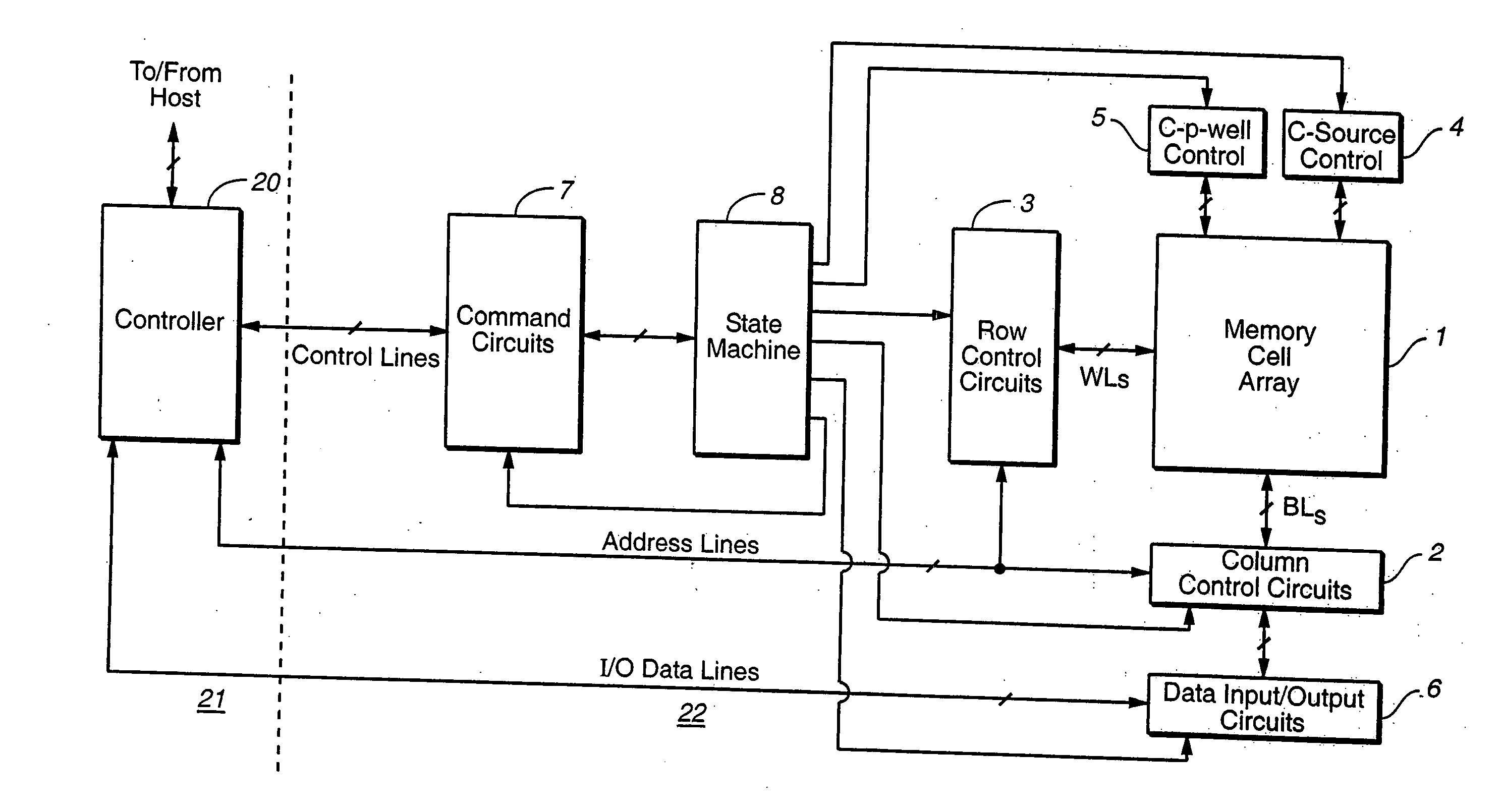
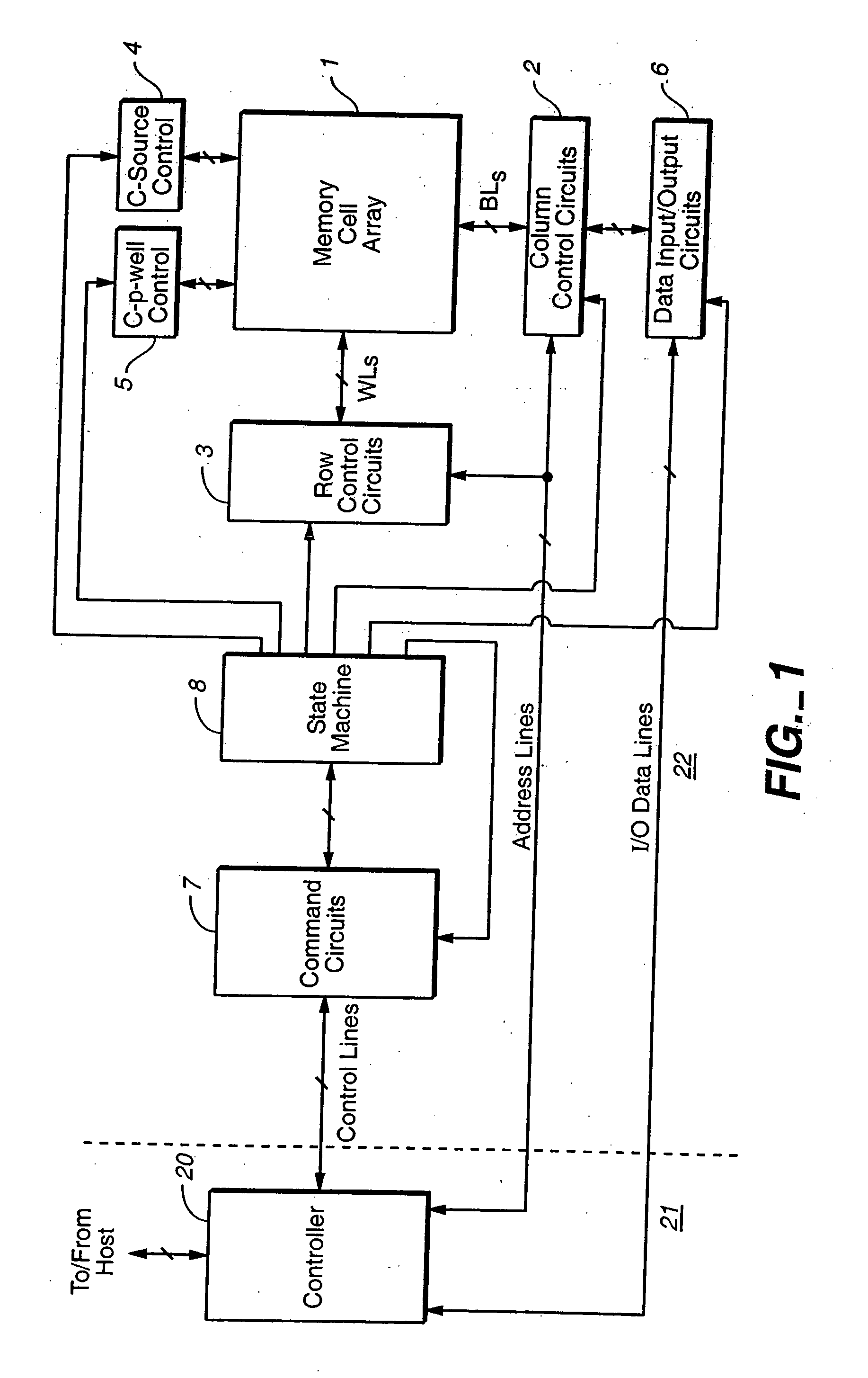
[0044] With reference to FIGS. 1-7, a specific non-volatile memory system is described in which the various aspects of the present invention are implemented, in order to provide specific examples. FIG. 1 is a block diagram of a flash memory system. Memory cell array 1 including a plurality of memory cells M arranged in a matrix is controlled by a column control circuit 2, a row control circuit 3, a c-source control circuit 4 and a c-p-well control circuit 5. The column control circuit 2 is connected to bit lines (BL) of the memory cell array 1 for reading data stored in the memory cells (M), for determining a state of the memory cells (M) during a program operation, and for controlling potential levels of the bit lines (BL) to promote the programming or to inhibit the programming. The row control circuit 3 is connected to word lines (WL) to select one of the word lines (WL), to apply read voltages, to apply a program voltages combined with the bit...


PUM


Abstract

A non-volatile memory system having an array of memory cells with at least one storage element each is operated with a plurality of storage level ranges per storage element. A flash electrically erasable and programmable read only memory (EEPROM) is an example, wherein the storage elements are electrically floating gates. The memory is operated to minimize the effect of charge coupled between adjacent floating gates, by programming some cells a second time after adjacent cells have been programmed. The second programming step also compacts a distribution of charge levels within at least some of the programming states. This increases the separation between states and / or allows more states to be included within a given storage window. An implementation that is described is for a NAND type of flash EEPROM.

Description

FIELD OF THE INVENTION [0001] This invention relates generally to a non-volatile memory and its operation, and, more specifically, to techniques for reducing the effects of data stored in one memory storage element upon data read from other storage elements. BACKGROUND OF THE INVENTION [0002] The principles of the present invention have application to various types of non-volatile memories, those currently existing and those contemplated to use new technology being developed. Implementations of the present invention, however, are described with respect to a flash electrically-erasable and programmable read-only memory (EEPROM), wherein the storage elements are floating gates. [0003] Field effect coupling between adjacent floating gates is described in U.S. Pat. No. 5,867,429 of Jian Chen and Yupin Fong, which patent is incorporated herein in its entirety by this reference. The degree of this coupling is necessarily increasing as the sizes of memory cell arrays are being decreased as...

Claims


Application Information

Patent Timeline
Patent Type & Authority Applications(United States)
IPC IPC(8): G11C16/02G11C11/56G11C16/00G11C16/04G11C16/12G11C16/34H01L21/8247H01L27/115H01L29/788H01L29/792
CPCG11C11/5621G11C11/5628G11C16/0483G11C16/3459G11C16/3404G11C16/3418G11C16/3454G11C16/12G11C16/00
Inventor CHEN, JIANTANAKA, TOMOHARUFONG, YUPINQUADER, KHANDKER N.
Owner TOSHIBA MEMORY CORP
Why Eureka
Try Eureka