Mechanically reconfigurable vertical tester interface for IC probing

Inactive Publication Date: 2005-12-15
FORMFACTOR INC
View PDF18 Cites 47 Cited by
  • Summary
  • Abstract
  • Description
  • Claims
  • Application Information

AI Technical Summary

Benefits of technology

[0020] Repositionable connectors are provided between the test head and probe card using a test head interface frame supporting the connectors. The position of the test head connectors can then be changed depending on whether full or partial wafer contact is desired. Such repositioning allows for an optimum connector arrangement to minimize sign

Problems solved by technology

When building semiconductor wafer contactor test systems, a major obstacle is the resource restrictions of a wafer tester.
The tester typically does not have enough resources or test channels to test all Devices U

Method used


Image

  • Mechanically reconfigurable vertical tester interface for IC probing
  • Mechanically reconfigurable vertical tester interface for IC probing
  • Mechanically reconfigurable vertical tester interface for IC probing

Examples


Embodiment Construction

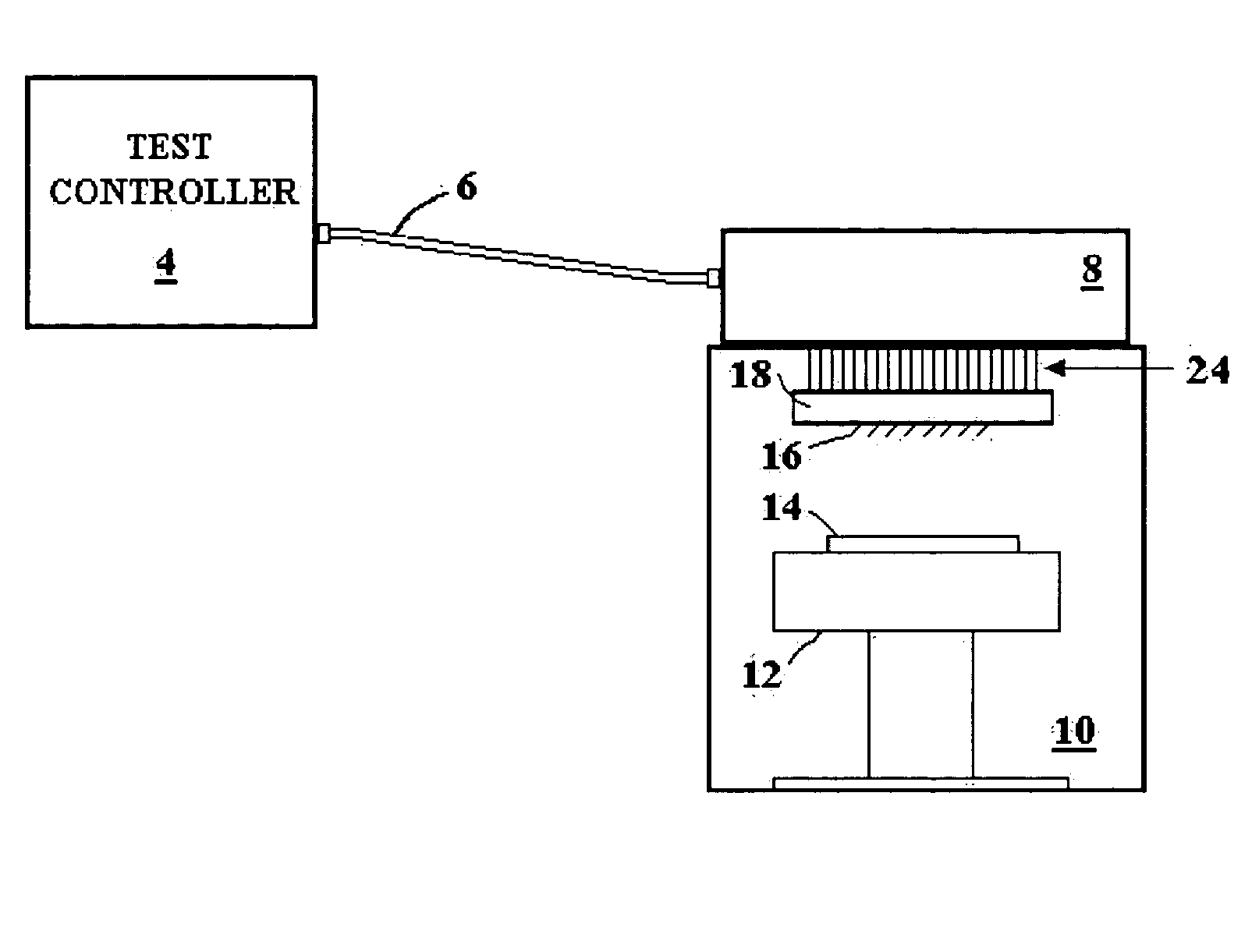
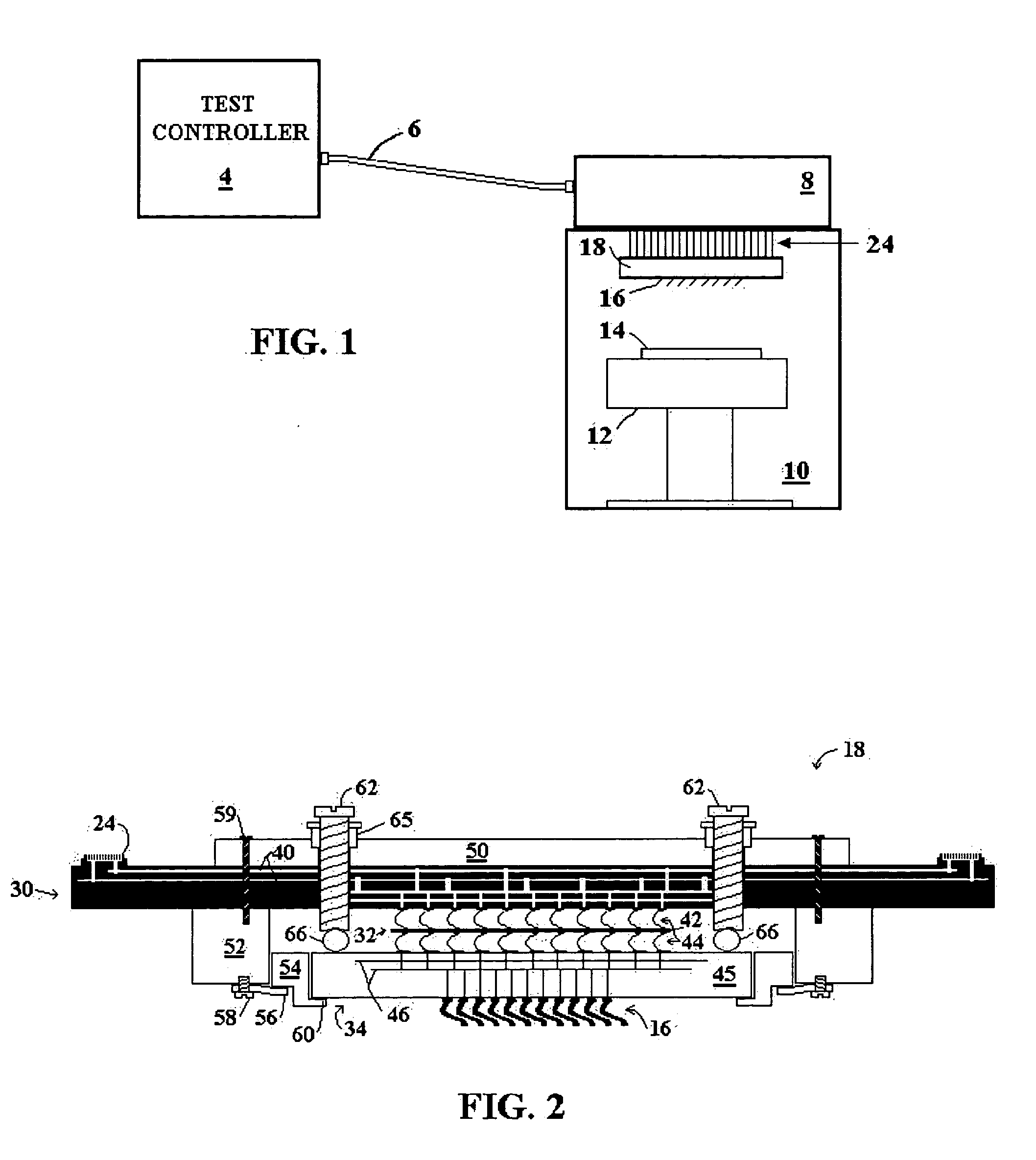
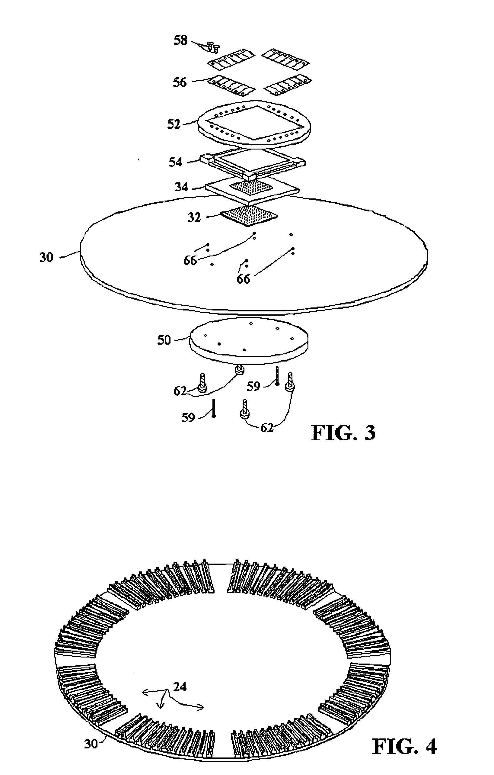
[0040]FIGS. 5A-5C illustrate how the probe head substrate can be segmented and arranged together as tiles in accordance with the present invention. FIG. 5A illustrates a substrate 71 over a wafer 73, where the substrate 71 that has not been segmented, while FIG. 5B illustrates a substrate segmented into quarters and FIG. 5C illustrates dividing a substrate into six parts. The substrates in FIGS. 5A-5C are further shown subdivided into device under test (DUT) sites each containing, for example, 10-200 probes for contacting corresponding pads or bumps of a single DUT on a wafer. A blowup of one DUT site 75 from substrate 71 of FIG. 5A shows a DUT site with eighteen contact elements.

[0041] The contact elements used may be spring probes, other contact elements for making electrical connections with DUTs on a wafer including without limitation needle probes, cobra style probes, buckling beam contacts, lithographically formed spring probes, elastomeric contacts, or rigid bumps, studs, po...


PUM


Abstract

A wafer test assembly includes multiple probe head substrates arranged like tiles with connectors attached to one side and probes supported on the opposing side. In one embodiment, flexible cable connectors directly connect the connectors on the probe head tile to a test head, while in another embodiment the flexible cables connect the probe head tile to a PCB providing horizontal routing to test head connectors. In one embodiment, leveling pins provide a simplified support structure connecting to a retaining element attached to the tiles to provide for applying a push-pull leveling force. A test head connector interface frame enables rearrangement of connectors between the test head and the probe card to provide for both full wafer contact or partial wafer contact. The test head connectors are rearranged by being slidable on rails, or pluggable and unpluggable enabling movement over a range of positions.

Description

BACKGROUND [0001] 1. Technical Field [0002] The present invention relates in general to a configuration of a test system for testing integrated circuits (ICs) on a wafer. More particularly, the present invention relates to the configuration of components of a probe card used in the wafer test system. [0003] 2. Related Art [0004] When building semiconductor wafer contactor test systems, a major obstacle is the resource restrictions of a wafer tester. The tester typically does not have enough resources or test channels to test all Devices Under Test (DUT) on a wafer. Because of the variety of numbers of DUTs on wafers, a given tester will likely be used both as a full wafer contact probe type interface, and an interface which contacts a portion of the wafer, referred to as a partial wafer probe. [0005] With an increased number of test channels, as well as increased size of wafers and the number of DUTs on a wafer, it becomes more desirable to modify the probe card for connecting the t...

Claims


Application Information

Patent Timeline
IPC IPC(8): G01R1/04G01R1/073G01R31/28H01R11/18
CPCG01R1/0416G01R31/2889G01R1/07307
Inventor ELDRIDGE, BENJAMIN N.VASQUEZ, BARBARASHINDE, MAKARAND S.MATHIEU, GAETAN L.SPORCK, A. NICHOLAS
Owner FORMFACTOR INC
Why Eureka
Try Eureka