Semiconductor device

a technology of semiconductor devices and devices, applied in semiconductor devices, semiconductor/solid-state device details, electrical apparatus, etc., can solve the problems of cracks on the bonding pad itself or on the lower face, lack of remedy for preventing cracks, and easy cracks on the bonding pad itself, so as to prevent corrosion of the interconnect and reduce the influence of cracks. , the effect of reducing the influence of the impa

Inactive Publication Date: 2005-12-22
RENESAS ELECTRONICS CORP
View PDF1 Cites 20 Cited by
  • Summary
  • Abstract
  • Description
  • Claims
  • Application Information

AI Technical Summary

Benefits of technology

[0021] In the region under the bonding pad, splitting the copper layer that is in contact with the bonding pad, into a section connected to the connection via plugs and a section connected to the seal ring, eliminates the possibility that an influence of a crack is propagated as far as to the section connected to the seal ring, even when the crack is produced in a region connected to the connection via plugs, which is considered to be the regions where a greatest portion of an impact force is applied, that is, the bonding pad or the copper layer connected to the bonding pad. Accordingly, such a structure effectively reduces the influence of the crack that may affect an interconnect located outside the seal ring.
[0022] The semiconductor according to the present invention allows absorbing an impact applied to a bonding pad during inspections before the shipment or in a positioning step for the wire bonding process, and securing a space for locating electronic components in a region under the bonding pad, still preventing corrosion of an interconnect due to possible intrusion of moisture through a crack produced in the bonding pad or an associated region, and further reducing the influence of the impact that may affect an interconnect extending to an external chip.

Problems solved by technology

An impact applied to the bonding pad at this moment may produce a crack in the bonding pad itself or on a lower face thereof.
Such a crack is more prone to appear, especially when a low dielectric constant film such as SiOC is employed.
However, although the semiconductor device according to the cited document is prone to produce a crack in relation with a bonding pad, this document does not provide any remedy for preventing the crack.
Therefore, the semiconductor device according to the cited document cannot be considered as reliable enough to locate electronic components in a region that undergoes an impact in the bonding process.
Also, intrusion of moisture through a crack produced by such an impact has to be addressed, as it may cause corrosion of an interconnect.

Method used


Image

  • Semiconductor device
  • Semiconductor device
  • Semiconductor device

Examples


first embodiment

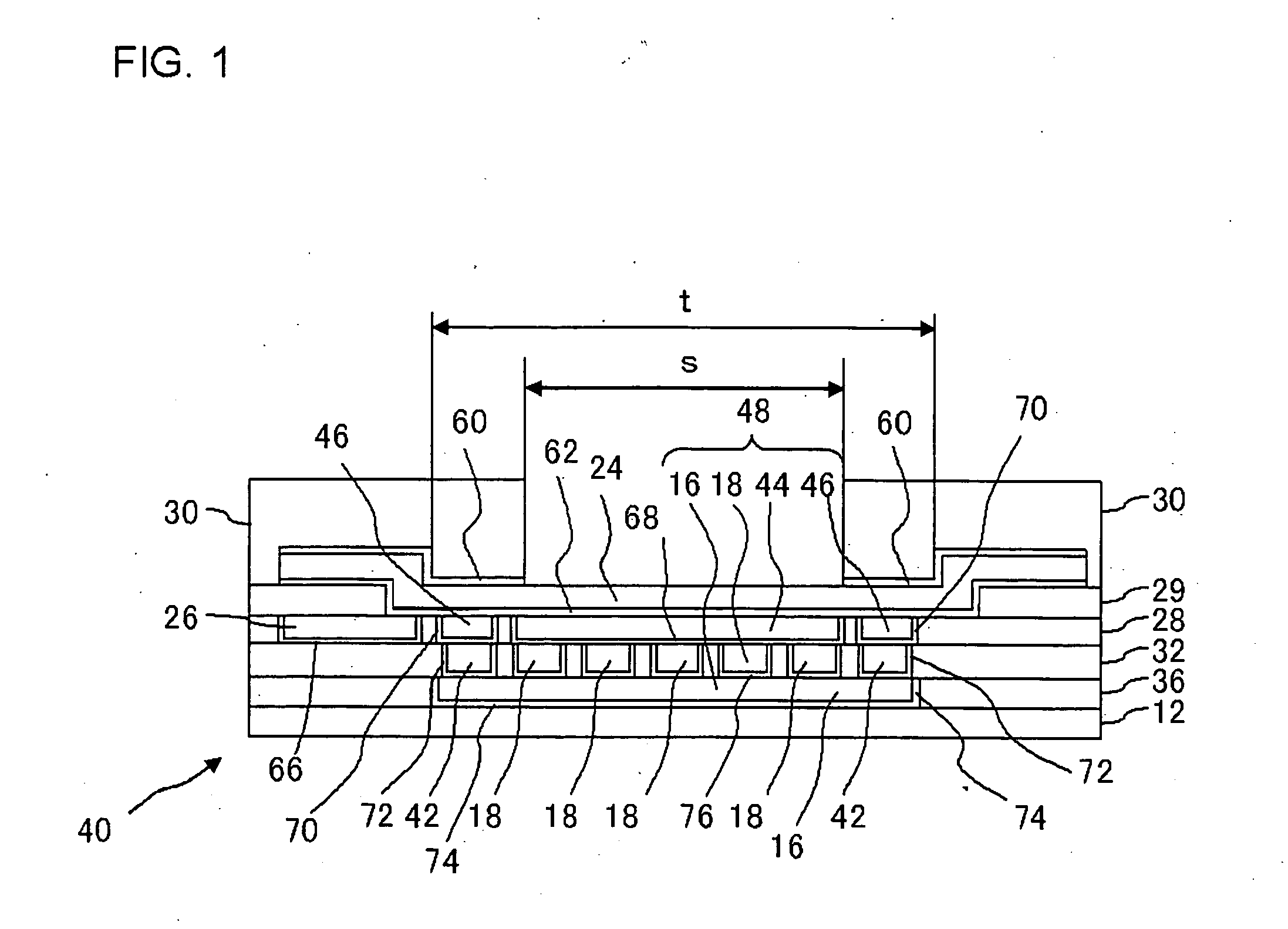
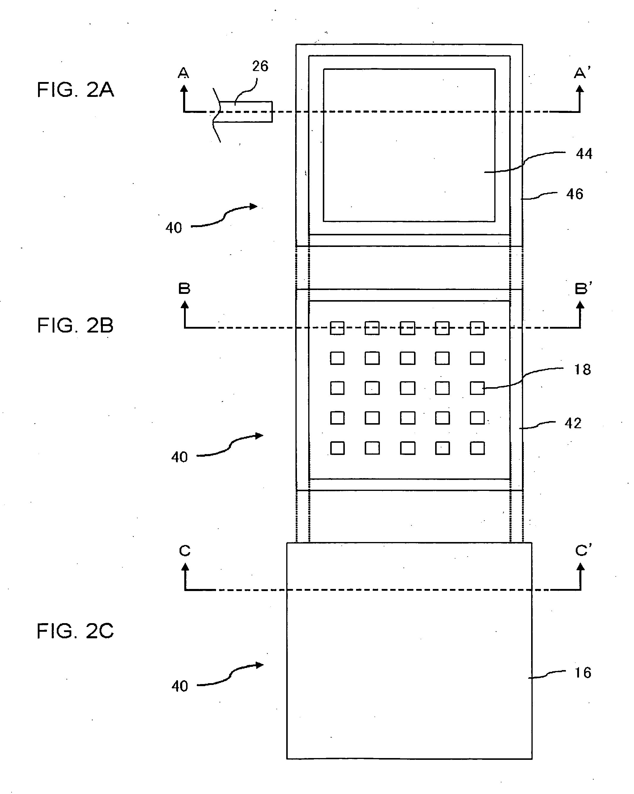
[0032]FIG. 1 is a schematic cross-sectional view showing a part a semiconductor device according to a first embodiment of the present invention, and FIGS. 2A to 2C are plan views showing interlayer dielectrics 28, 32 and 34, respectively, according to the first embodiment.

[0033] The semiconductor device according to this embodiment includes a bonding pad 24 serving as an external connection terminal, a region (under the bonding pad) 48 including, under the bonding pad 24, a first copper layer 44 and a second copper layer 16 located under the bonding pad 24, corresponding to at least two copper layers, as well as connection via plugs 18 provided so as to connect the first copper layer 44 and the second copper layer 16, a seal ring 42 constituted of an annular conductor disposed so as to surround the region under the bonding pad 48, and connecting the second copper layer 16, which is the lower copper layer in the pair, to the first copper layer 44, which forms a pair with the second ...

second embodiment

[0071]FIG. 5 is a schematic cross-sectional view showing a part a semiconductor device according to a second embodiment of the present invention.

[0072] A semiconductor device 10 according to the second embodiment has basically the same structure as the semiconductor device 40 according to the first embodiment shown in FIG. 1. A difference is that the first copper layer 44 and the seal ring copper layer 46, separately formed in the insulating interlayer 28 in the first embodiment, are continuously formed to constitute a unified first copper layer 22.

[0073] Also, the semiconductor device 10 can be fabricated through substantially the same steps as those taken in the first embodiment.

[0074] Providing thus a region under the bonding pad 34, including the first copper layer 22, a plurality of connection via plugs 18 and the second copper layer 16 so as to directly contact the lower face of the bonding pad 24 allows absorbing an impact imposed by inspections before the shipment and by ...

third embodiment

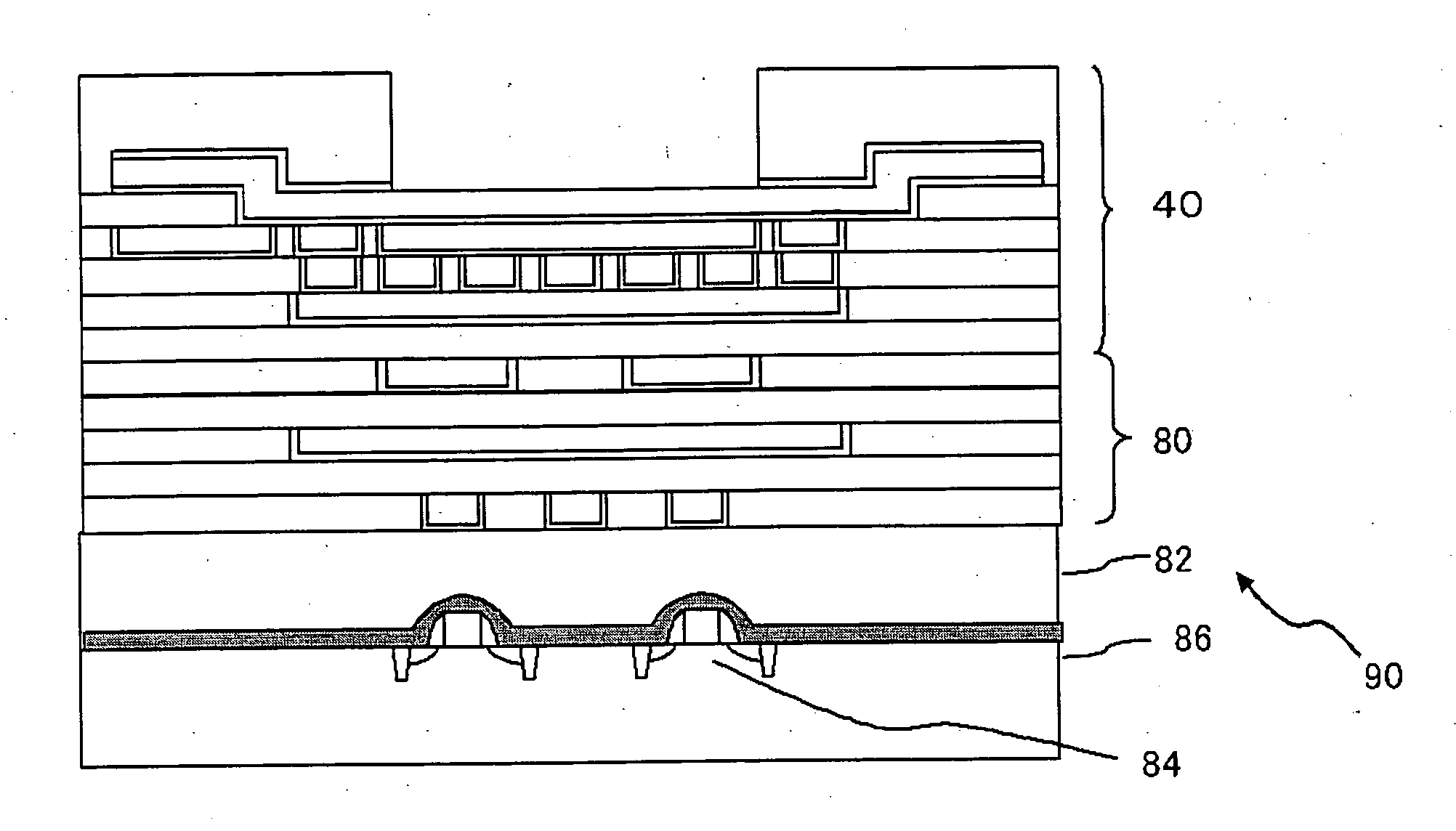
[0078]FIG. 6 is a schematic cross-sectional view showing a part of a semiconductor device according to a third embodiment of the present invention.

[0079] A semiconductor device 90 according to the third embodiment includes a multilayer interconnect 80 disposed under the semiconductor device 40 according to the first embodiment, and a silicon substrate 86, which serves as the base substrate of this semiconductor device, disposed in contact with a lower face of a lowermost insulating interlayer 82. In the silicon substrate 86, an MOS (metal oxide semiconductor) 84 which is an electronic device, may be located at a position corresponding to the opening of the semiconductor device 40 serving as an external connection terminal.

[0080] As described above, the semiconductor device 40 according to this embodiment is sufficiently reliable for locating electronic components right under the bonding pad. Employing the semiconductor device 40 as a section to constitute a bonding pad for connect...


PUM


Abstract

A semiconductor device should have a structure that allows locating electronic components in a region under a bonding pad. The semiconductor device includes a bonding pad constituting the external connection terminal; a region under the bonding pad including at least two copper layers and a connection via plug, under said bonding pad, disposed so as to connect copper layers that form a pair out of the at least two copper layers; a seal ring constituted of an annular conductor, disposed so as to surround the region under the bonding pad, and to connect a lower one of the copper layers that form said pair to copper layer to form a pair with the lower copper layer; and an interconnect connected to the bonding pad outside the seal ring.

Description

[0001] This application is based on Japanese patent application No. 2004-180628, the content of which is incorporated hereinto by reference. BACKGROUND OF THE INVENTION [0002] 1. Field of the Invention [0003] The present invention relates to a semiconductor device, and more particularly to a semiconductor device including an external connection terminal disposed on a semiconductor substrate. [0004] 2. Description of the Related Art [0005] One of semiconductor devices that stand a stress or an impact applied to a bonding pad when performing a wire bonding process, despite a narrow spacing between the bonding pads, is disclosed in JP-A No. 2001-267323. [0006] The cited document discloses a semiconductor device including a dummy interconnect located in an insulating interlayer, so that a bonding pad is directly sustained by the dummy interconnect. SUMMARY OF THE INVENTION [0007] The bonding pad is subjected to various inspections before shipment of the finished product, and besides whe...

Claims


Application Information

Patent Timeline
Patent Type & Authority Applications(United States)
IPC IPC(8): H01L23/48H01L23/485
CPCH01L24/03H01L2224/02166H01L2224/05082H01L2224/05093H01L2224/05095H01L2224/05096H01L2224/05181H01L2224/05187H01L2224/05567H01L2224/05624H01L2924/01004H01L2924/01005H01L2924/01006H01L2924/01013H01L2924/01014H01L2924/01029H01L2924/01073H01L2924/01078H01L2924/01082H01L2924/04953H01L2924/05042H01L24/05H01L2924/0002H01L2924/01033H01L2924/04941H01L2924/00014H01L2224/05552
Inventor TSUTSUI, YUTAKAOKADA, NORIO
Owner RENESAS ELECTRONICS CORP
Why Eureka
Try Eureka