Contact pad arrangement for integrated SD/MMC system

a contact pad and integrated technology, applied in the direction of printed circuit aspects, electrical apparatus construction details, electrical apparatus casings/cabinets/drawers, etc., can solve the problems of sd cards, inability to fit in mmc slots, etc., to facilitate the fabrication of memory cards and facilitate the accurate positioning of contact pads during assembly and use.

Inactive Publication Date: 2005-12-22
SUPER TALENT ELECTRONICS
View PDF28 Cites 74 Cited by
  • Summary
  • Abstract
  • Description
  • Claims
  • Application Information

AI Technical Summary

Benefits of technology

[0009] The present invention is directed to printed circuit boards (PCBs) having contact pads arranged in a novel 13-pad configuration that facilitates the fabrication of memory cards meeting both the Secure-Digital (SD) and MultiMediaCard (MMC) form factors, thereby facilitating an integrated SD / MMC system in which a given PCB may be used to produce a memory card based on either the SD or the MMC electronic protocols. The present invention is also directed to 13-pad memory cards that are fabricated using the novel 13-pad configuration, along with various alignment features that greatly facilitate accurate positioning of the contact pads during assembly and use.

Problems solved by technology

MMC cards can fit in SD slots, but SD cards, which are packaged in about 50% thicker housings, cannot fit in MMC slots.
One limitation to the 9-pad form factor is that data is transferred in a parallel x4-bit manner (i.e., four bits per transmission cycle).

Method used


Image

  • Contact pad arrangement for integrated SD/MMC system
  • Contact pad arrangement for integrated SD/MMC system
  • Contact pad arrangement for integrated SD/MMC system

Examples


Embodiment Construction

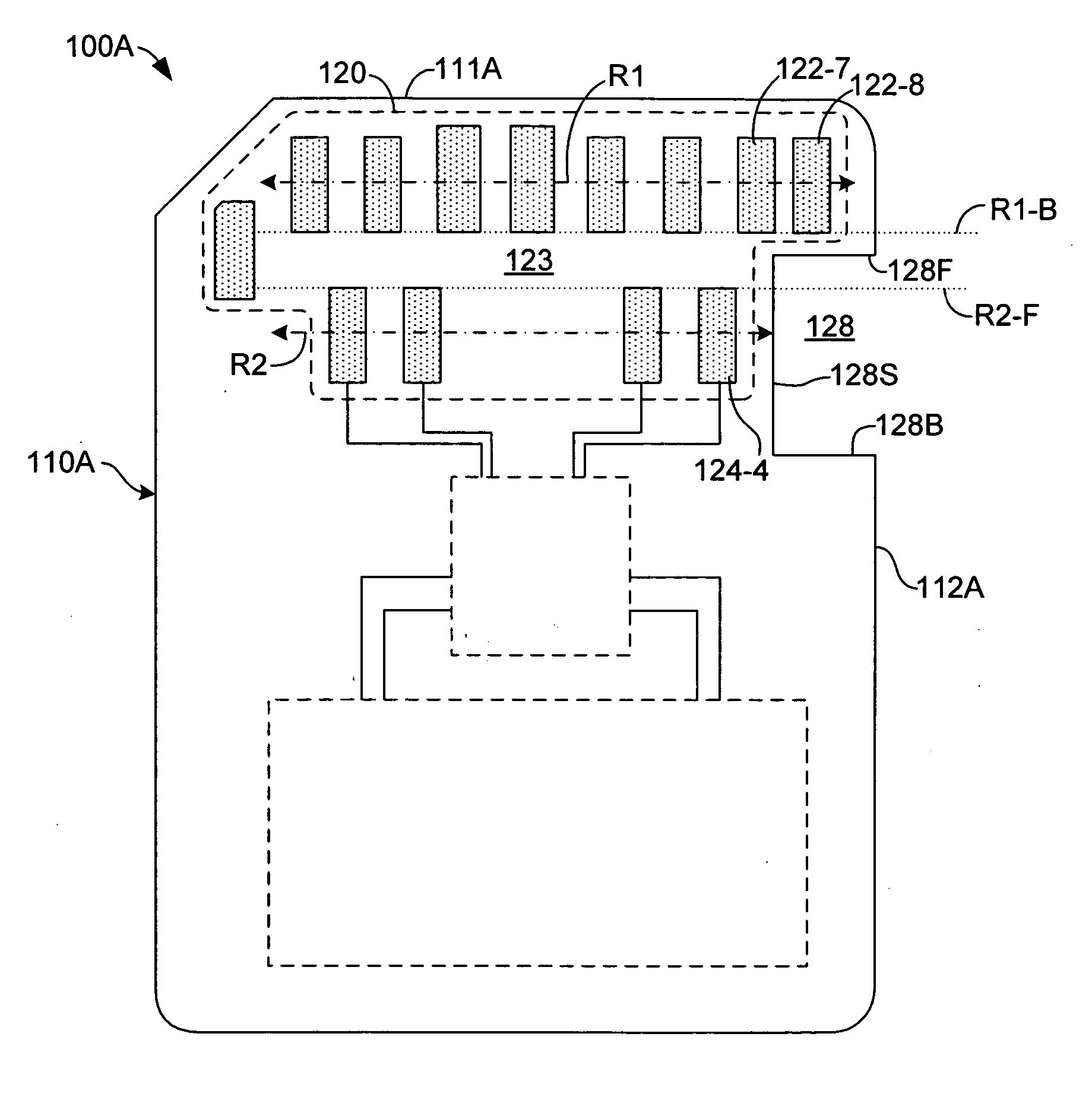
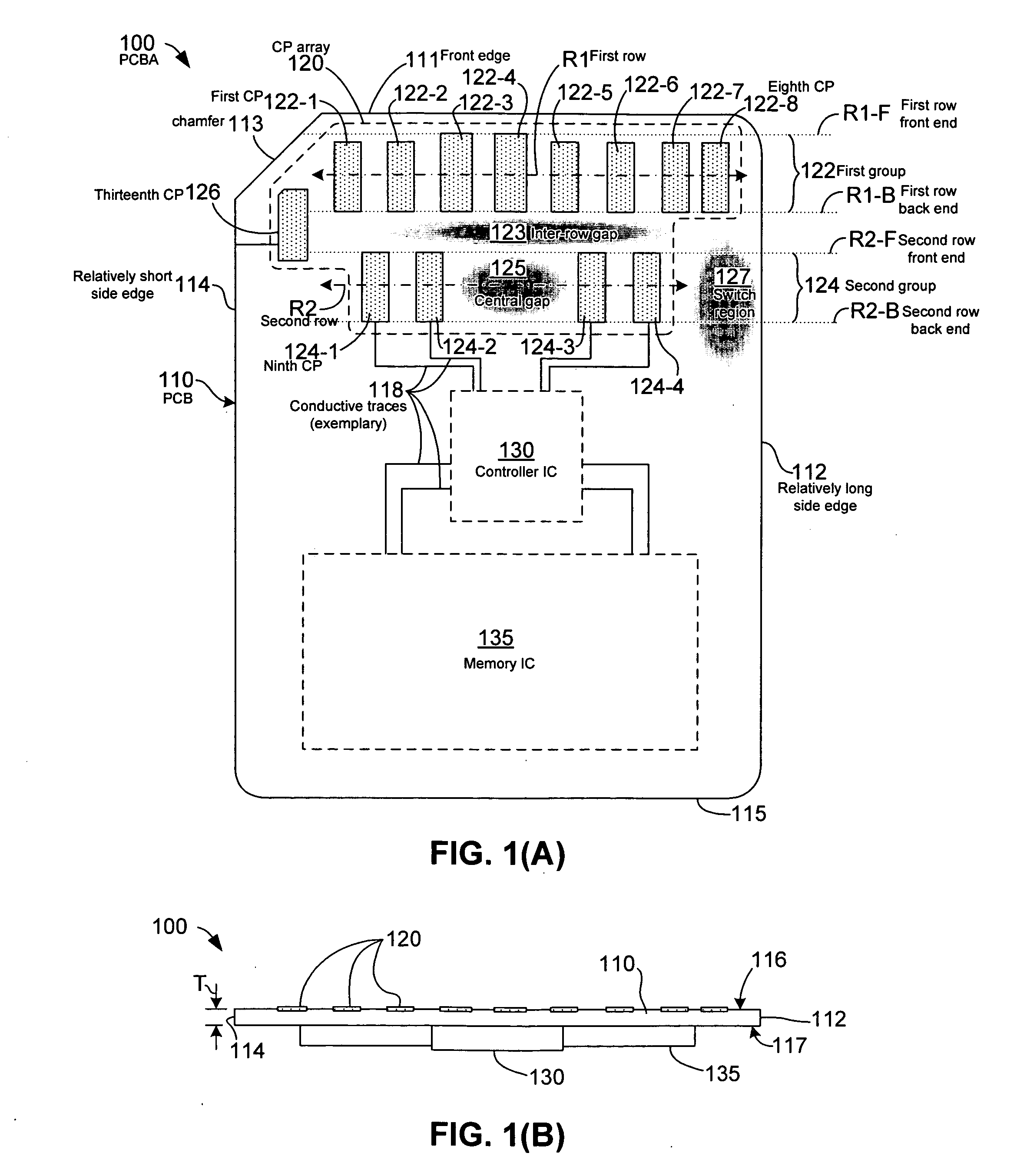
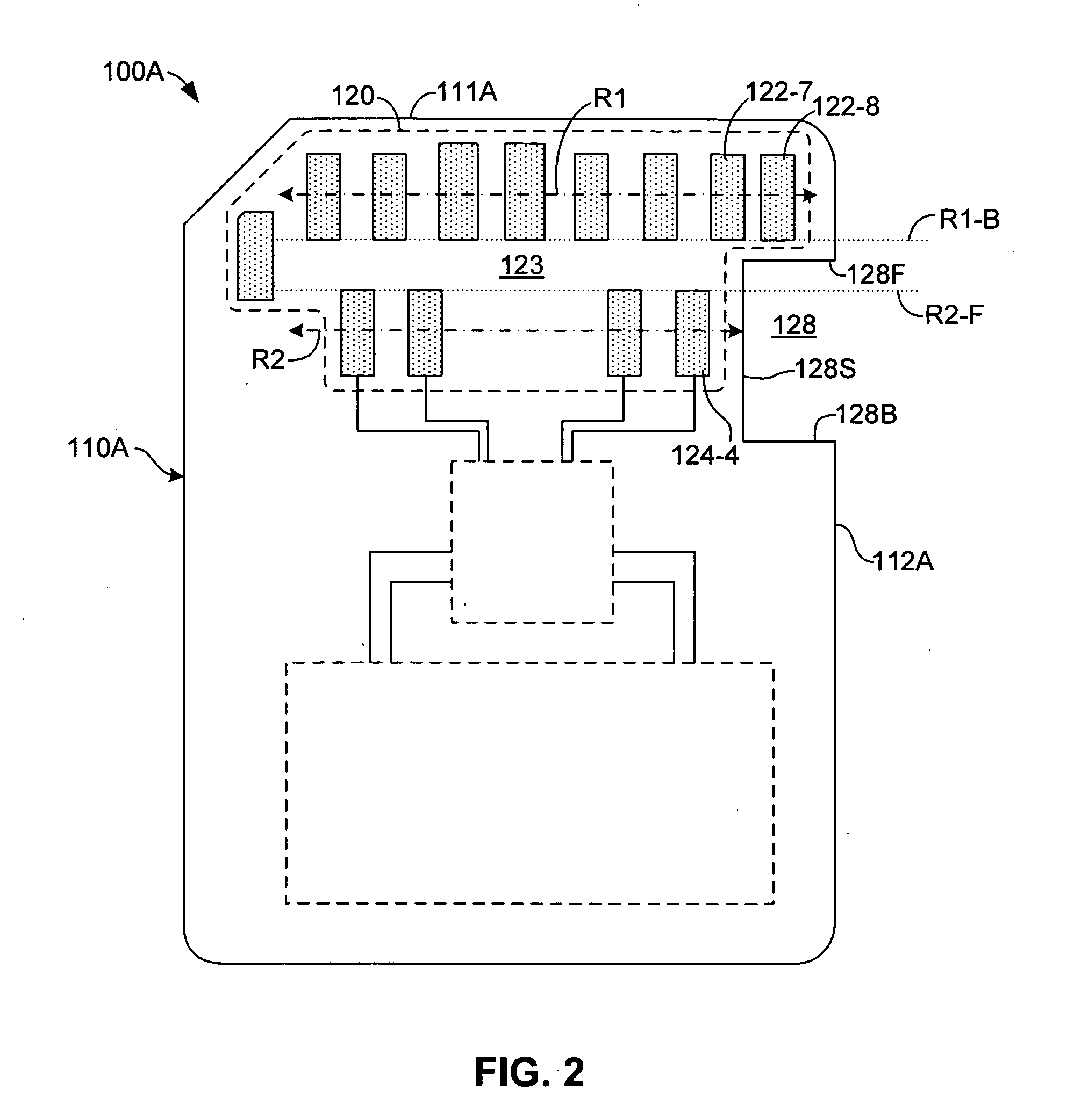
[0028] FIGS. 1(A) and 1(B) are top plan and end elevation views showing a printed circuit board assembly (PCBA) 100 for a 13-pad memory card according to an embodiment of the present invention. PCBA 100 generally includes a printed circuit board (PCB) 110 having a contact pad array 120 mounted on a first (e.g., upper) surface thereof, and one or more integrated circuits (ICs) 130 and 135 mounted on a second (e.g., lower) surface thereof. PCB 110 is formed in accordance with known PCB manufacturing techniques such that the contact pads of array 120 and ICs 130 and 135 (as well as other circuit components, which are omitted for brevity) are electrically interconnected by a predefined network of conductive traces 118 (only a few of which are shown for illustrative purposes).

[0029] PCB 110 is a substantially rectangular, flat substrate including multiple layers of conductive traces 118 and other conducting structures sandwiched between multiple layers of an insulating material (e.g., F...


PUM


Abstract

A memory card having thirteen contact pads arranged on a PCB in a manner that supports an integrated SD/MMC system. Eight contact pads form a front row, four contact pads form a second row behind the front row, and a thirteenth contact pad is located between the front and back rows adjacent to a chamfer formed on the PCB. An L-shaped gap region is provided between the first and second rows, and between the second row and side edge of the PCB. An optional alignment notch is defined along the side edge adjacent the second row. An optional alignment hole is defined between adjacent contact pads of the second row that receives an alignment pin passing between two covers of a two-part housing. The memory card electronics are compatible with either the MMC or SD protocols, and the housing is consistent with either the MMC or SD mechanical form factors.

Description

BACKGROUND OF THE INVENTION [0001] 1. Field of the Invention [0002] This invention relates to removable memory cards, and more particularly to removable memory cards for dual-protocol systems. [0003] 2. Related Art [0004] Flash-memory cards are widely used for storing digital pictures captured by digital cameras. One useful format is the Secure-Digital (SD) format, which is an extension of the earlier MultiMediaCard (MMC) format. Such memory cards are also useful as add-on memory cards for other devices, such as portable music players, personal digital assistants (PDAs), and even notebook computers. SD cards are hot-swappable, allowing the user to easily insert and remove SD cards without rebooting or cycling power. Since the SD cards are small, durable, and removable, data files can easily be transported among electronic devices by being copied to an SD card. SD cards are not limited to flash-memory cards, but other applications such as communications transceivers can be implemente...

Claims


Application Information

Patent Timeline
Patent Type & Authority Applications(United States)
IPC IPC(8): H05K1/11H05K5/04H05K7/06
CPCH05K1/117H05K2201/09063H05K2203/167H05K2201/09409H05K2201/09145
Inventor WANG, KUANG-YUNI, JIMSEE, SUN-TECK
Owner SUPER TALENT ELECTRONICS
Why Eureka
Try Eureka