

Multiple signal format output buffer
- Summary
- Abstract
- Description
- Claims
- Application Information
AI Technical Summary
Benefits of technology
Problems solved by technology
Method used
Image

Examples
Embodiment Construction
)
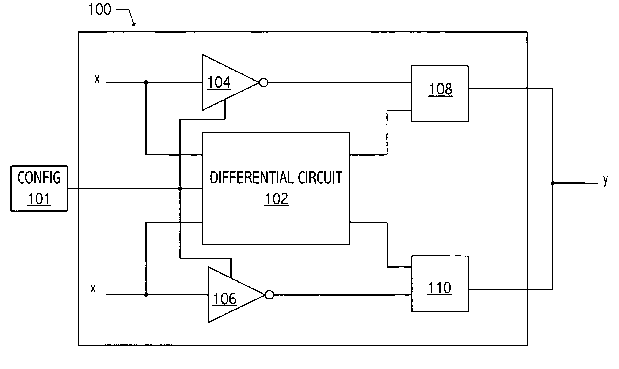
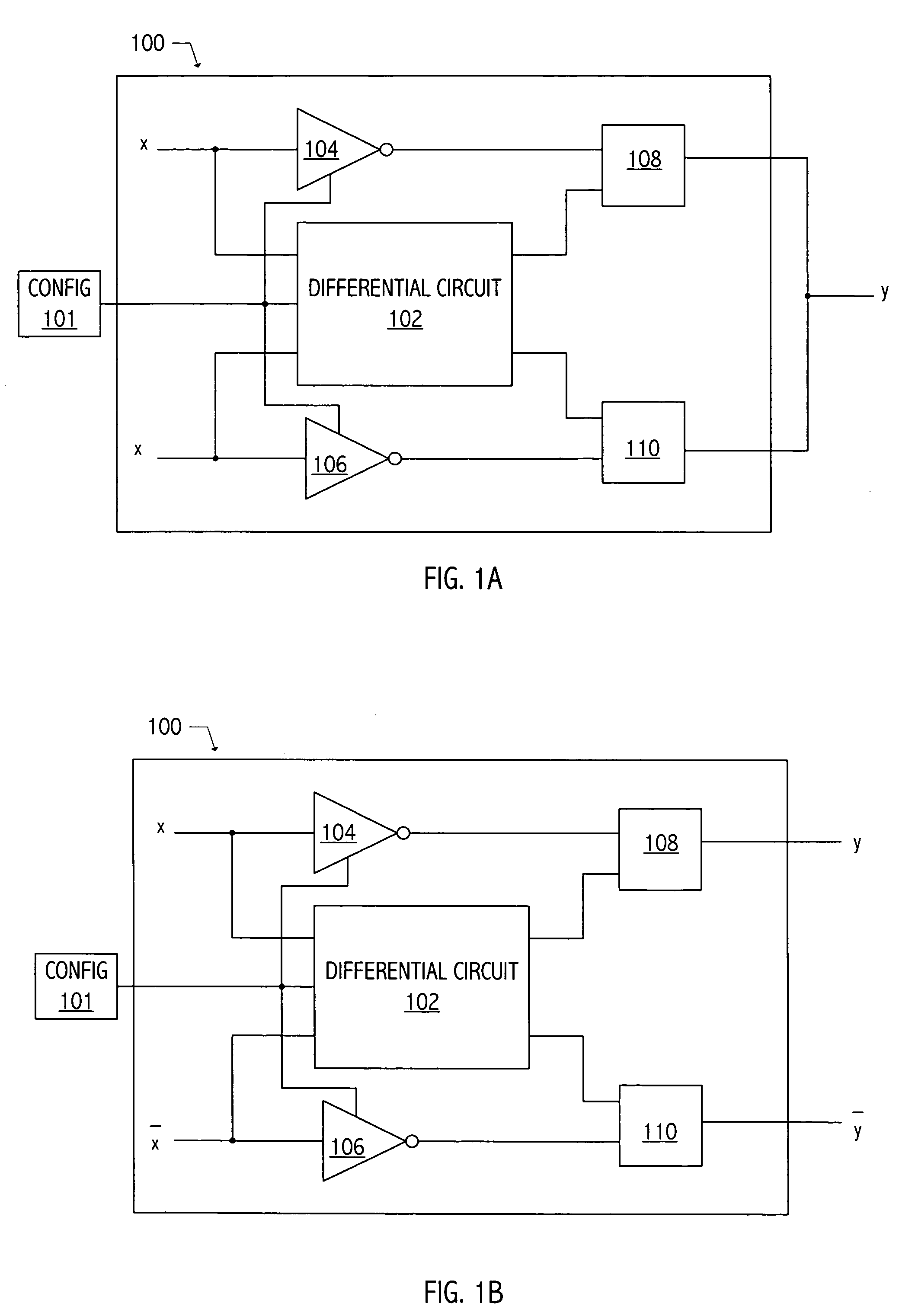
[0027]FIGS. 1A and 1B illustrate integrated circuit 100, which may be an output portion of a microprocessor, a clock source integrated circuit, or other integrated circuit product. Integrated circuit 100 supports a CMOS mode, i.e., a single-ended mode, a mode in which a single input signal produces a single output, e.g., as configured in FIG. 1A. Integrated circuit 100 also supports a differential mode, i.e., a differential input produces a differential output, e.g., as configured in FIG. 1B. The mode of integrated circuit 100 may be selected by configuration block 101, e.g., digital logic, non-volatile memory control, or other suitable technique. In the CMOS mode, the inputs received by CMOS drivers 104 and 106 are in phase, as illustrated by the input ‘x’, which drives both CMOS driver 104 and 106 to produce an output ‘y’. In the differential mode, the inputs received by differential circuit 102 are out of phase, as illustrated by the input ‘x’ and ‘{overscore (x)}’, which drive ...
PUM
 Abstract
Description
Claims
Application Information