Driving circuit including shift register and flat panel display device using the same

a technology of shift register and display device, which is applied in the direction of static storage, digital storage, instruments, etc., can solve the problems of large volume, heavy weight, and drawbacks of crts

Active Publication Date: 2005-12-29
LG DISPLAY CO LTD
View PDF9 Cites 76 Cited by
  • Summary
  • Abstract
  • Description
  • Claims
  • Application Information

AI Technical Summary

Benefits of technology

[0026] An advantage of the present invention is to provide a driving circuit that sequentially outputs signals of various shapes and a flat panel display device including such a driving circuit.
[0027] Another advantage of the invention is to provide a method of driving a flat panel display device that sequentially outputs signals of various shapes.
[0028] Additional features and advantages of the invention will be set forth in the description which follows, and in part will be apparent from the description, or may be learned by practice of the invention. These and other advantages of the invention will be realized and attained by the structure particularly pointed out in the written description and claims hereof as well as the appended drawings.
[0029] To achieve these and other advantages and in accordance with the purpose of the present invention, as embodied and broadly described, a driving circuit for a flat panel display device includes a generation unit for generating n-phase form generation clocks; and a plurality of shift register stages for sequentially generating a plurality gate signals to a plurality of gate lines using the n-phase form generation clocks, one of the shift register stage including first and second output terminals for outputting first and second switching signals, respectively, using an output signal of one of the preceding shift register stages and an output signal of one of the subsequent shift register stages; a first transistor connected to the first output terminal for receiving one of the n-

Problems solved by technology

However, CRTs have some drawbacks such as heavy weight, large volume and high driving voltage.
In addition, the shape of the output signals may not be modified once the related art shift regis

Method used


Image

  • Driving circuit including shift register and flat panel display device using the same
  • Driving circuit including shift register and flat panel display device using the same
  • Driving circuit including shift register and flat panel display device using the same

Examples


first embodiment

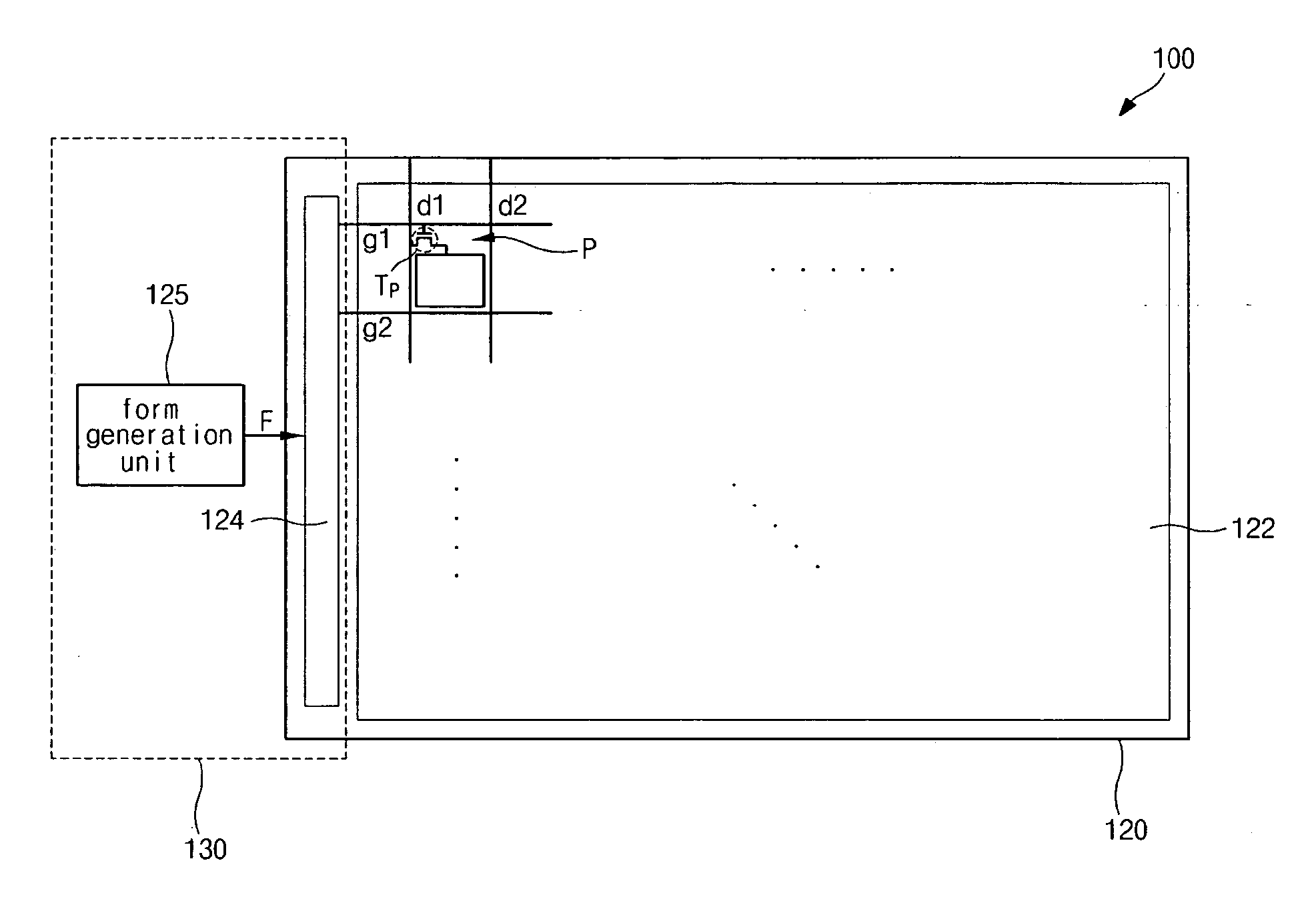
[0060]FIG. 9 is a schematic circuit diagram illustrating a driving circuit in a display panel for a flat panel display device according to the present invention.

[0061] As illustrated in FIG. 9, the driving circuit includes a plurality of shift register stages “SRS1,”“SRS2”, “SRS3” and “SRS4”. For the sake of brevity, only four shift register stages are shown and explained. Each of the shift register stages “SRS1,”“SRS2”, “SRS3” and “SRS4” includes a shift register unit “SRU1,”“SRU2”, “SRU3” or “SRU4”, a first transistor “T1” and a second transistor “T2”, and a first AND operator “A1” and a second AND operator “A2”. An RS flip-flop circuit is used for the shift register units “SRU1,”“SRU2”, “SRU3” and “SRU4”, and an AND gate circuit is used for the first and second operators “A1” and “A2”. Each of the shift register stages “SRS 1,”“SRS2”, “SRS3” and “SRS4” is connected to the corresponding gate line “g1”, “g2”, “g3” or “g4”. An array resistor R and an array capacitor C connected to e...

second embodiment

[0106] FIGS. 21 to 23 are schematic timing charts showing three examples of signals input to and output from the driving circuit of FIG. 20 according to the present invention.

[0107] As shown in FIGS. 21 to 23, three-phase form generation clocks “F1” to “F3” have wave shapes “WS1” to “WS3” corresponding to the four-phase form generation clocks of FIGS. 10 to 12, respectively, except for a period of the form generation clock. In other words, because the three-phase form generation clocks “F1” to “F3” are input to the corresponding shift register stages, the period “T2” of the three-phase form generation clocks “F1” to “F3” is less than the period “T1” of the four-phase form generation clocks. In these examples, the period “T2” is equal to ¾“T1”. The output signals of the driving circuit can have a variety of shapes even after the driving circuit is formed by providing clock signals having a variety of shapes to the driving circuit. Accordingly, a fixation problem of output signal shap...


PUM


Abstract

A driving circuit for a flat panel display device includes a generation unit for generating n-phase form generation clocks; and a plurality of shift register stages for sequentially generating a plurality gate signals to a plurality of gate lines using the n-phase form generation clocks, one of the shift register stage including first and second output terminals for outputting first and second switching signals, respectively, using an output signal of one of the preceding shift register stages and an output signal of one of the subsequent shift register stages; a first transistor connected to the first output terminal for receiving one of the n-phase form generation clocks; and a second transistor connected to the second output terminal and the first transistor, wherein each gate line is connected to a node between the first and second transistors.

Description

[0001] The present invention claims the benefit of Korean Patent Application No. 2004-0049526, filed in Korea on Jun. 29, 2004, which is hereby incorporated by reference for all purposes as if fully set forth herein. BACKGROUND OF THE INVENTION [0002] 1. Field of the Invention [0003] The present invention relates to a display device and a method of driving a display device, and more particularly, to a liquid crystal display (LCD) device and a method of driving an LCD device. [0004] 2. Discussion of the Related Art [0005] Cathode ray tubes (CRTs) are used for display devices such as televisions and monitors. However, CRTs have some drawbacks such as heavy weight, large volume and high driving voltage. Accordingly, flat panel display (FPD) devices having advantages of portability and low power consumption have been the subject of much recent research and development for the coming information era. Among the various types of FPD devices, liquid crystal display (LCD) devices and electro...

Claims


Application Information

Patent Timeline
IPC IPC(8): G09G3/36
CPCG09G3/3677G09G2310/0267G11C19/184G09G2310/06G09G2310/0286G09G3/20G09G3/30G09G3/36G11C19/28
Inventor JANG, YONG-HOYOON, SOO-YOUNGCHO, NAM-WOOK
Owner LG DISPLAY CO LTD
Why Eureka
Try Eureka