Leadframe with a chip pad for two-sided stacking and method for manufacturing the same

a chip pad and two-sided stacking technology, applied in the field of leadframes, can solve the problems of not being able to meet the requirements of multi-chip layout, affecting the layout of leadframes, and reducing the number of chips packed inside the molding compound, so as to achieve no complexity

Inactive Publication Date: 2005-12-29
ADVANCED SEMICON ENG INC
View PDF4 Cites 13 Cited by
  • Summary
  • Abstract
  • Description
  • Claims
  • Application Information

AI Technical Summary

Benefits of technology

[0007] It is therefore a main object of the invention to provide a leadframe with a chip pad for two-sided stacking. The leadframe includes a chip pad and a plurality of leads. A dielectric adhesive layer is used to fix a first trace layer onto the lower surface of the chip pad. At least a through hole passes through the chip pad, the dielectric adhesive layer and the first trace layer. An electrically-conductive material is formed inside the through hole, so that the connecting pad of the first trace layer is electrically connected to the chip pad. The electronic component mounted on the lower surface of the chip pad can be electrically connected to the chip pad for the bonding wire to connect the upper surface of the chip pad to the leads for achieving two-sided stacking of the chip pad. The upper and the lower surface of chip pad are effectively used and no complexity is added to the manufacturing process of wire-bonding.
[0008] It is therefore a second object of the invention to provide a multi-chip package structure of a chip pad for two-sided stacking. The multi-chip package structure includes a chip pad and a plurality of leads both of which are components of a leadframe. A dielectric adhesive layer and a first trace layer are formed on the lower surface of the chip pad. At least a through hole passes through the chip pad, the dielectric adhesive layer and the first trace layer. An electrically-conductive material is formed inside the through hole for the connecting pad of the first trace layer to be electrically connected to the chip pad, and a solder mask is formed on the first trace layer. A surface mounting electronic component or another chip can be mounted on the lower surface of the chip pad to be electrically connected to the connecting pad of the first trace layer, so that the bonding wire on the upper surface of the chip pad electrically connects the connecting pad of the first trace layer to the leads for achieving a multi-chip package which is easy to achieve high-intensity trace and easy to manufacture, and capable of integrating various electronic components under the chip pad.

Problems solved by technology

However, as the conductive path of the chips inside the package becomes more complicated, it becomes more difficult for the layout of the leads of the leadframe to meet the requirements of the multi-chip.
Moreover, the number of the chips packed inside a molding compound is limited, the layout of trace can not be too complicated due to the leadframe and bonding wire, neither can a passive piece nor other surface mounting electronic component be integrated into the upper and the lower surface of the chip pad.

Method used


Image

  • Leadframe with a chip pad for two-sided stacking and method for manufacturing the same
  • Leadframe with a chip pad for two-sided stacking and method for manufacturing the same
  • Leadframe with a chip pad for two-sided stacking and method for manufacturing the same

Examples


Embodiment Construction

[0015] Referring to the accompanying drawings, the invention is exemplified by the embodiment disclosed below.

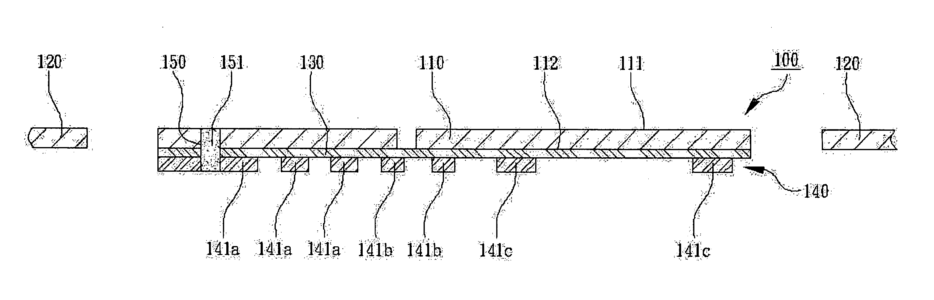
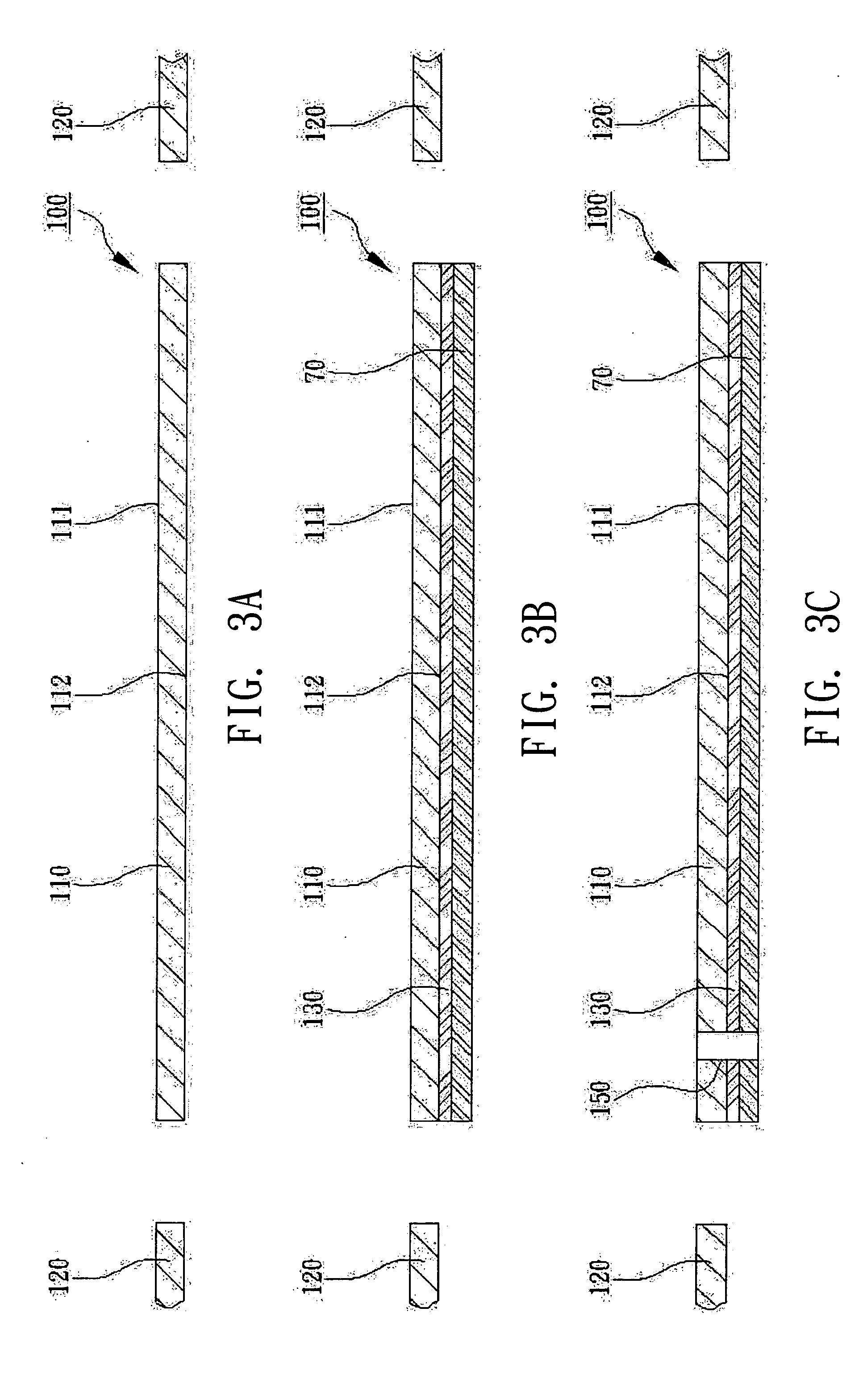
[0016] Referring to FIG. 2 a cross-sectional view of a leadframe with a chip pad for two-sided stacking according to an embodiment of the invention is shown. A leadframe with a chip pad for two-sided stacking 100 mainly includes a chip pad 110, a plurality of leads 120, a dielectric adhesive layer 130, a first trace layer 140, at least a through hole 150 and an electrically-conductive material 151. The chip pad 110 and the leads 120 have the same metal material. The chip pad 110 has an upper surface 111 and a lower surface 112. The leads 120 are disposed on 110 the periphery of the chip pad. The dielectric adhesive layer 130 is formed on the lower surface 112 of the chip pad 110 to adhere the first trace layer 140 onto the lower surface 112 of the chip pad 110. The first trace layer 140 is disposed on the dielectric adhesive layer 130 but is not directly electrically connec...


PUM


Abstract

A leadframe with a chip pad for two-sided stacking including a chip pad and a plurality of leads is disclosed. A dielectric adhesive layer is formed on the lower surface of the chip pad and is adhered onto a first trace layer, which has a connecting pad. At least a through hole passes through the chip pad, the dielectric adhesive layer and the first trace layer. An electrically-conductive material is formed inside the through hole for electrically connecting the connecting pad of the first trace layer to the chip pad. When an electronic component is mounted on the lower surface of the chip pad, a plurality of bonding wires having one ends on the upper surface of the chip pads can electrically connect the electronic component to the leads for achieving two-sided stacking of the chip pad.

Description

[0001] This application claims the benefit of Taiwan application Serial No. 93119078, filed Jun. 29, 2004, the subject matter of which is incorporated herein by reference. BACKGROUND OF THE INVENTION [0002] 1. Field of the Invention [0003] The invention relates in general to a leadframe, and more particularly to a leadframe with a chip pad for two-sided stacking and the manufacturing method for the same. [0004] 2. Description of the Related Art [0005] Multi-chip package (MCP), a packaging technology attracting more and more attentions recently, integrates several chips of various types or passive pieces into a semiconductor package structure, so that the MCP is more available in functions or higher in capacity. A leadframe with chip pad is a commonly used multi-chip carriage and is conducive to the saving of manufacturing costs. Besides, in order to further reduce package size, a chip or a passive piece is respectively stacked on the upper and the lower surface of the chip pad of th...

Claims


Application Information

Patent Timeline
Patent Type & Authority Applications(United States)
IPC IPC(8): H01L21/44H01L21/48H01L21/50H01L23/495H01L25/065H01L25/16
CPCH01L23/49575H01L2224/73265H01L25/16H01L2224/16H01L2224/48091H01L2224/48137H01L2224/48247H01L2924/19105H01L2924/19106H01L2924/19107H01L25/0652H01L24/48H01L2224/32245H01L2924/00014H01L2924/00H01L2924/12042H01L2924/181H01L2924/00012H01L2224/45099H01L2224/45015H01L2924/207
Inventor HUANG, YAO-TING
Owner ADVANCED SEMICON ENG INC
Why Eureka
Try Eureka