Lockstep mechanism to ensure security in hardware at power-up

a technology of hardware and security, applied in the field of lockstep mechanism to ensure security in hardware at power-up, can solve the problems of consuming valuable circuit board real estate, unable to allow a bed of nails tester to directly access the package connection, and leadless surface mount packages,

Inactive Publication Date: 2005-12-29
QUALCOMM INC
View PDF9 Cites 130 Cited by
  • Summary
  • Abstract
  • Description
  • Claims
  • Application Information

AI Technical Summary

Benefits of technology

[0006] A secure electronic device and method of securing access to a communication port of an electronic device, such as a JTAG test interface in an ASIC are disclosed. The device may be secured from physical attacks by initializing the port in a disabled or otherwise severely limited state. The configured accessibility of the port may be enabled when the device receives a non-secure access key vector. The ASIC compares the received non-secure access key vector against an internally stored access key and enables the communication port in the ASIC if a predetermined relationship exists between the two. As part of enabling the communication port, the ASIC may perform an initialization routine and may selectively enable access via the communication port in response to a predetermined access configuration. The access configuration may be determined based in part on states of one or more fuses within the ASIC.

Problems solved by technology

Leadless surface mount packages, such as Ball Grid Array (BGA) packages, do not allow a bed of nails tester to directly access the package connections.
However, these test pads or lands consume valuable circuit board real estate and impede a designer's ability to effectively miniaturize a circuit board.
In high speed electronic circuits, the test pads or lands may adversely affect the performance of the circuit.
Moreover, as IC's incorporate increased functionality, the ability to physically probe logical blocks becomes infeasible.
Because the JTAG interface can be configured to provide access to all logical structures and registers within a device, secure devices can be compromised via an attack executed using the JTAG interface.
Additionally, because a service provider can charge for downloaded files, the downloaded files are typically encrypted before being transmitted and are also typically encrypted when stored in the non-volatile memory to reduce the possibility of a user redistributing the downloaded file.
Unfortunately, boundary scan testing, such as JTAG testing, allows access to internal logic within a device, such as an ASIC.
Eliminating boundary scan access to the logic containing the hardware key can greatly limit the scope of testing and verification that may be performed on the ASIC.
However, providing unlimited access to the internal logic of the ASIC can severely compromise the integrity of the secure hardware key.

Method used


Image

  • Lockstep mechanism to ensure security in hardware at power-up
  • Lockstep mechanism to ensure security in hardware at power-up
  • Lockstep mechanism to ensure security in hardware at power-up

Examples


Embodiment Construction

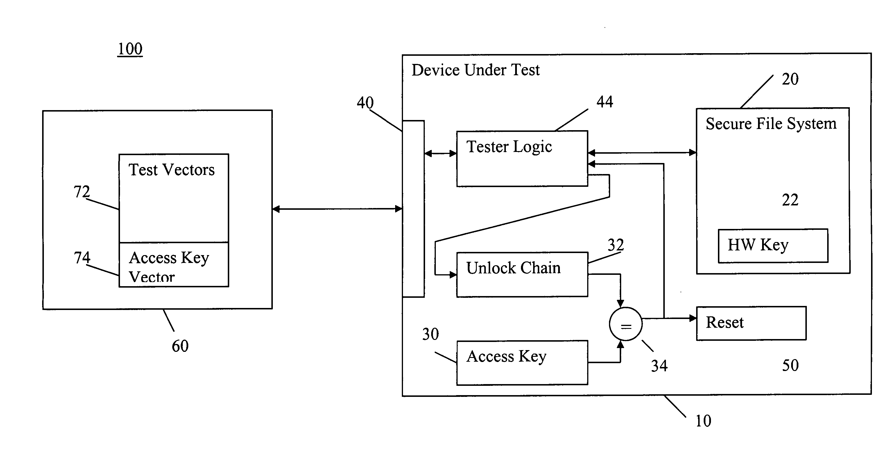
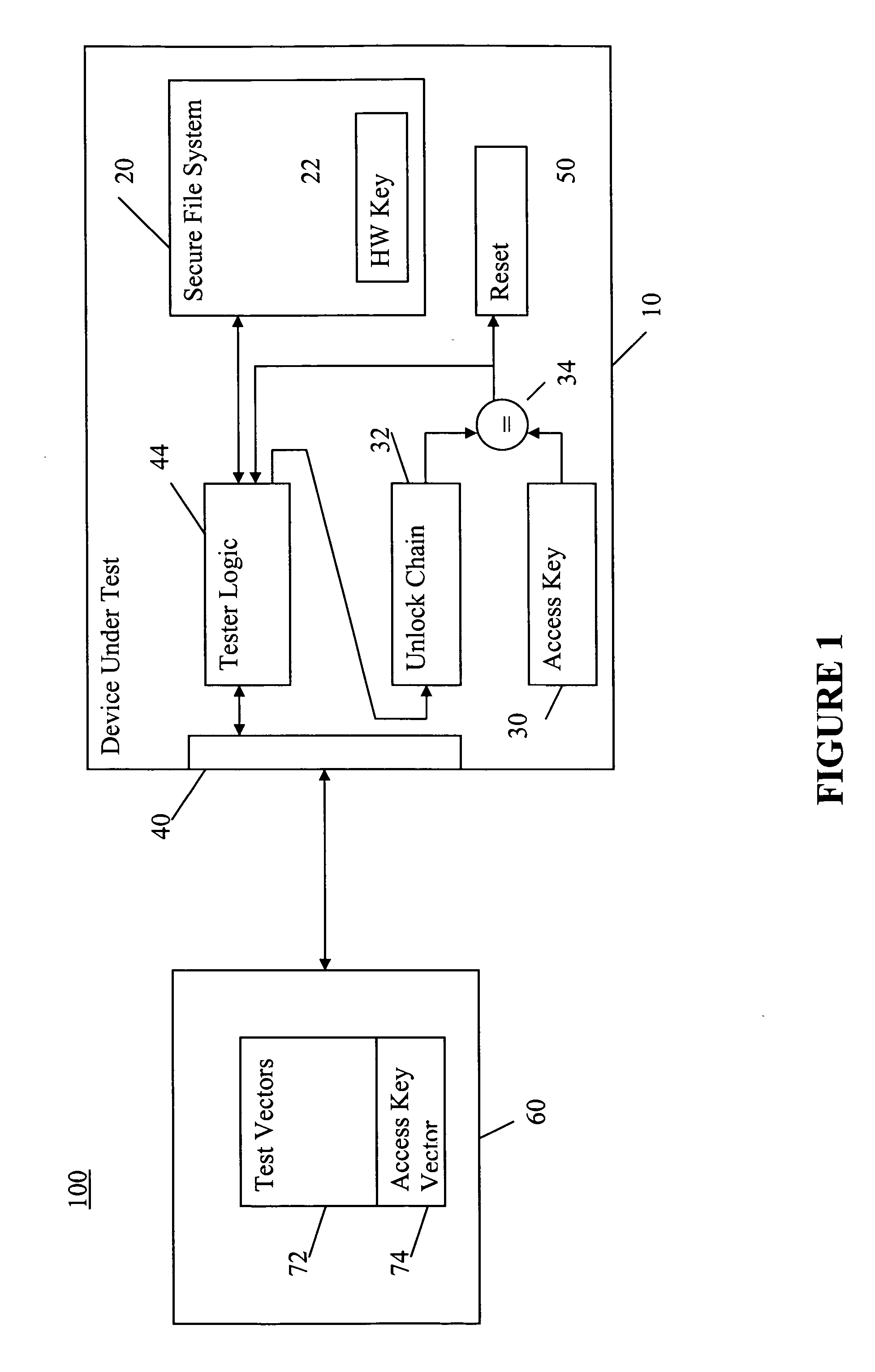
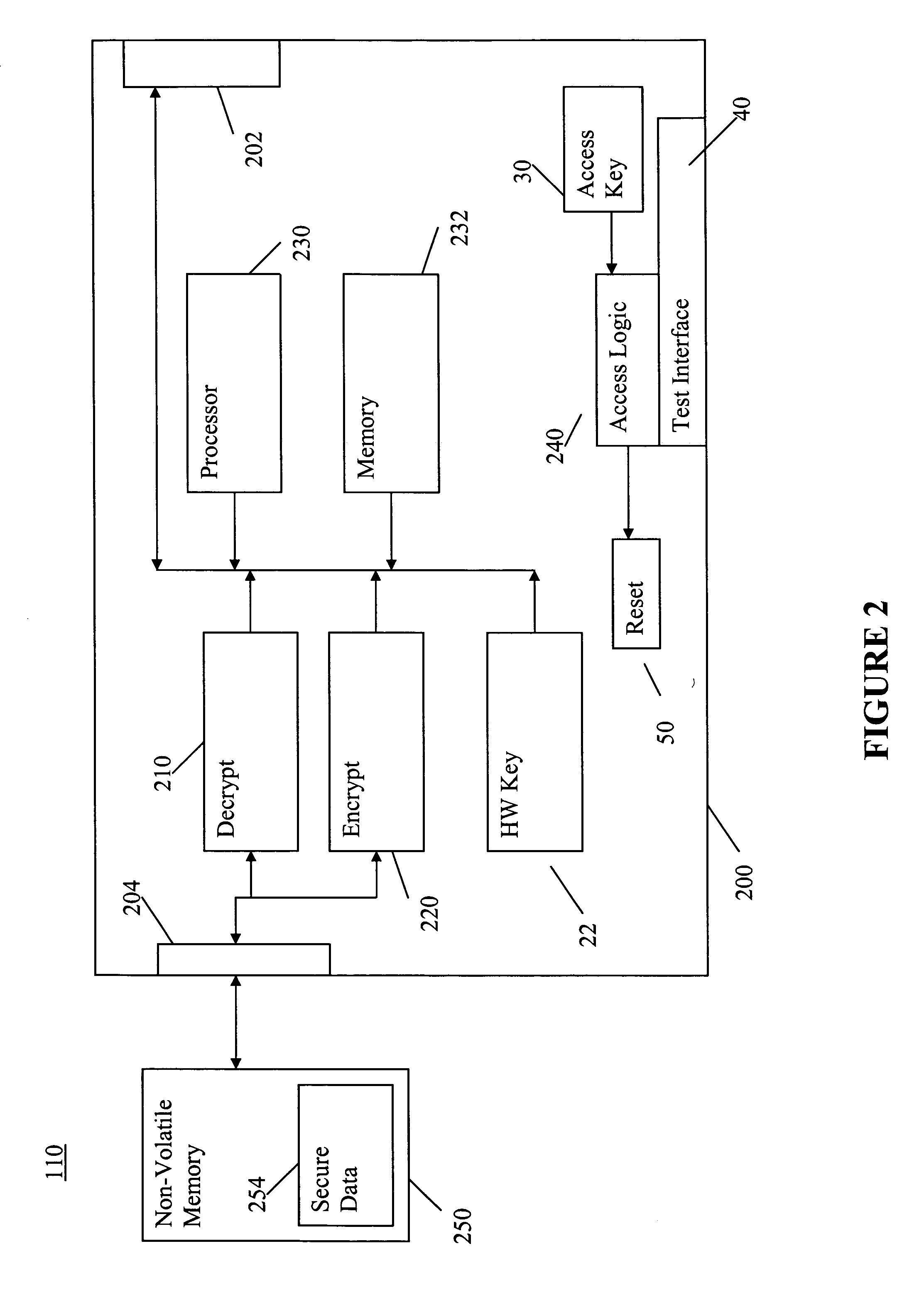
[0016] A secure device, such as an ASIC having a secure hardware key stored in a register, can limit access to secure portions of the device using one or more fuses that can be selectively blown. The state of the fuses may be read and corresponding chip access may be enabled or disabled based on the state of the fuses. Upon initial energization or power-up of the ASIC, the state of one or more of the fuses may be floating, random, or otherwise indeterminate. Alternatively, the state of the logic that senses the fuse states may be initialized in a random or otherwise non-functioning state and may not be able to read the fuse states until after the chip performs an initialization process that is normally part of the power-on reset routine. The fuses, or alternatively the circuits that read the fuse states, may be initialized as part of a power-on reset process to ensure their proper states. The result of either the fuse states initializing in a random state, or the sensing logic initi...


PUM


Abstract

A system and method of ensuring hardware security of a device, such as an integrated circuit having secure data stored thereon. The integrated circuit or other hardware device can implement one or more configurable fuses that limit access to one or more secure locations within the device. The secure locations may contain secure data. The state of the configurable fuses can be ensured, thereby limiting access to secure locations, by forcing the occurrence of a logical state prior to allowing access to hardware locations configured by the fuses. A configurable non-secure access code can be used to force the occurrence of the logical state. Receipt of the non-secure access code by the hardware device forces the occurrence of the hardware state, thereby ensuring access only to those secure locations configured by the fuses.

Description

BACKGROUND OF THE DISCLOSURE [0001] Various device and circuit board designs are used in the struggle to continually miniaturize consumer electronics. Integrated circuits (IC's) used in circuit boards have migrated from through-hole packages to leaded surface mount packages, and then to leadless surface mount packages. Leadless surface mount packages, such as Ball Grid Array (BGA) packages, do not allow a bed of nails tester to directly access the package connections. In some cases, circuit board designers implement conductive pads or lands that allow a connection to a bed of nails tester. However, these test pads or lands consume valuable circuit board real estate and impede a designer's ability to effectively miniaturize a circuit board. In high speed electronic circuits, the test pads or lands may adversely affect the performance of the circuit. Moreover, as IC's incorporate increased functionality, the ability to physically probe logical blocks becomes infeasible. [0002] A varie...

Claims


Application Information

Patent Timeline
Patent Type & Authority Applications(United States)
IPC IPC(8): G01R31/317G01R31/3185H04K1/00H04L9/00
CPCG01R31/318536G01R31/31719G01R31/317G01R31/3185
Inventor KITARIEV, DIMITRISHIPPEE, GEOFFREYVARADARAJAN, SRINIVAS
Owner QUALCOMM INC
Why Eureka
Try Eureka