IC-tag-bearing wiring board and method of fabricating the same

a wiring board and tag technology, applied in the direction of printed circuit aspects, circuit inspection/indentification, printed electric component incorporation, etc., can solve the problems of reducing the packaging efficiency of electronic parts, the inability of ic tag-bearing wiring boards to be manufactured, and the inability to mount electronic parts in parts of the top layer corresponding to the parts of the inner layer in which the antenna pattern is formed, etc., to achieve accurate receipt and high packaging efficiency

Inactive Publication Date: 2006-01-05
HITACHI LTD
View PDF8 Cites 200 Cited by
  • Summary
  • Abstract
  • Description
  • Claims
  • Application Information

AI Technical Summary

Benefits of technology

[0010] According to the present invention, the antenna of the radio IC tag is formed in the side surface of the wiring board. Therefore, the first and the second major surface of the wiring board can be effectively used for mounting electronic parts on the wiring board, and electronic parts can be mounted on the first major surface of the wiring board in a high packaging efficiency.
[0011] Since the directivity of the antenna in a desired direction can be controlled by the auxiliary antenna formed on the first or the second major surface of the wiring board, signals provided by the IC chips of the radio IC tags of a plurality of stacked IC tag-bearing wiring boards can be accurately received and information about the wiring boards can be read.

Problems solved by technology

Although the technique previously disclosed in JP Heisei 11-515094 forms antenna patterns in parts of the inner layers of the multilayer printed wiring board, electronic parts cannot be mounted in a part of the top layer corresponding to the parts of the inner layers in which the antenna patterns are formed.
Thus the antenna of the radio IC tag formed on the first or the second major surface of the printed wiring board reduces electronic part packaging efficiency.
The conventional IC tag-bearing wiring board is unable to meet contradictory conditions respectively requiring maintaining a desired communication ability and improving electronic part packaging efficiency.
In an electronic apparatus provided with a plurality of stacked IC tag-bearing wiring boards, radio waves radiated by the antennas of the stacked IC tag-bearing wiring boards interfere with each other, and, in some cases, information provided by a desired one of those IC tag-bearing wiring boards cannot be identified.

Method used


Image

  • IC-tag-bearing wiring board and method of fabricating the same
  • IC-tag-bearing wiring board and method of fabricating the same
  • IC-tag-bearing wiring board and method of fabricating the same

Examples


first embodiment

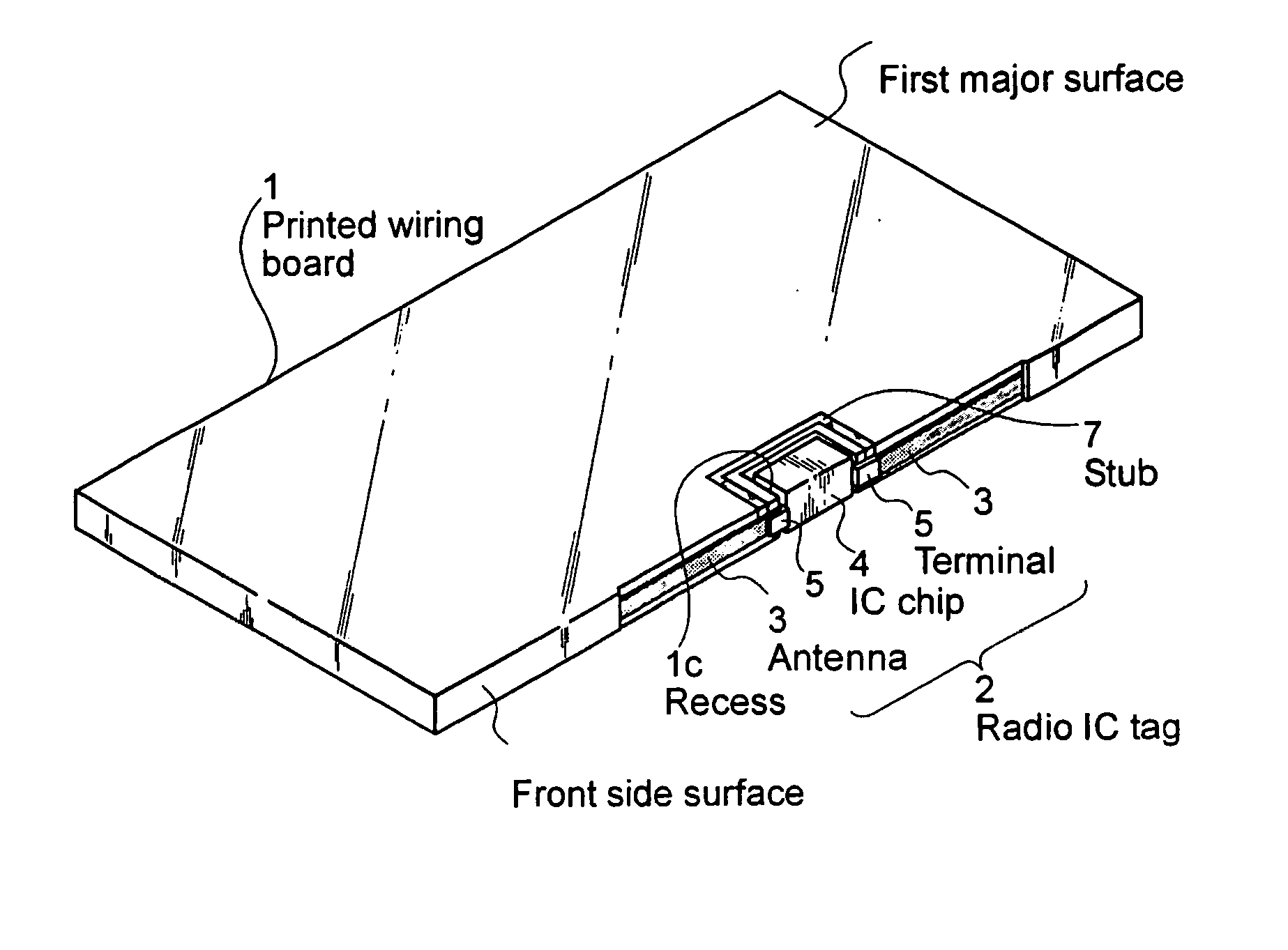
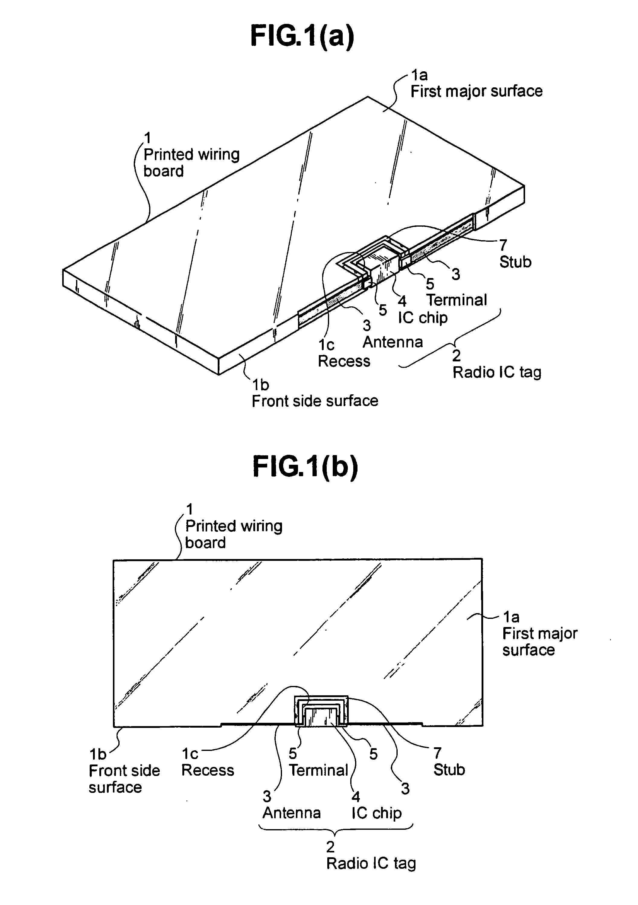
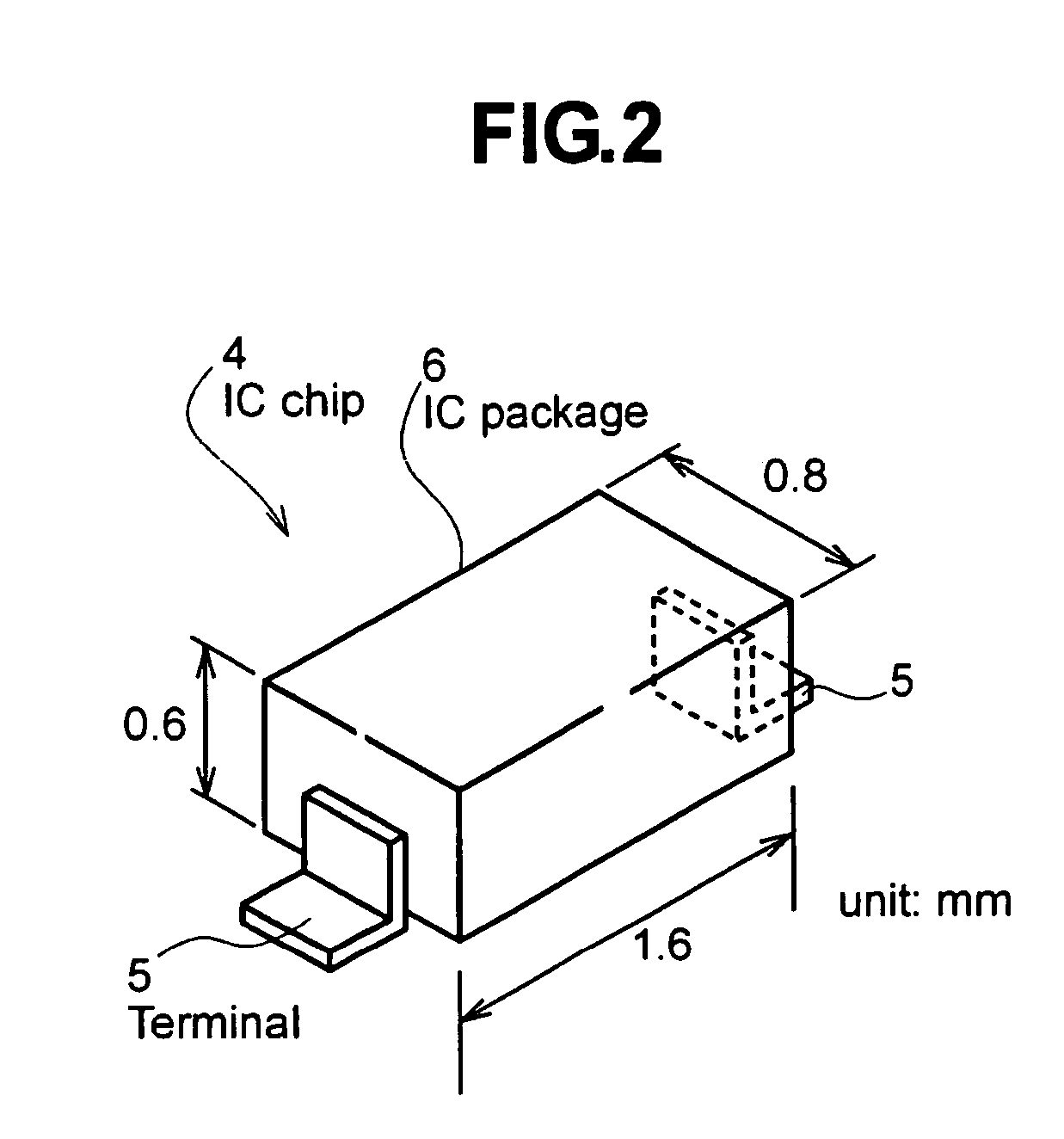
[0027] FIGS. 1(a) and 1(b) are a front perspective view and a top view, respectively, of an IC tag-bearing wiring board in a first embodiment according to the present invention. Referring to FIGS. 1(a) and 1(b), a recess 1c is formed in a middle part of the front side surface 1b of a printed wiring board 1, and an antenna 3 consisting of two antenna elements formed on the front side surface 1b so as to extend on the opposite sides of the recess 1c, respectively. The antenna 3 is a dipole antenna of a length equal to λ / 2, where λ is the wavelength of radio waves to be radiated by the antenna. The antenna 3 of λ / 2 in length radiates radio waves having a wavelength of λ at a maximum radiation efficiency. An IC chip 4 is placed in the recess 1c formed between the two antenna elements of the antenna 3. The antenna elements of the antenna 3 are connected electrically to terminals 5 of the IC chip 4. Many electronic parts, not shown, are mounted on a first major surface 1a of the printed w...

second embodiment

[0036] FIGS. 4(a) and 4(b) are a front perspective view and a top view, respectively, of an IC tag-bearing wiring board in a second embodiment according to the present invention. As shown in FIG. 4(a), an antenna 3a may be formed so as to extend from the front side surface 1b and a first major surface 1a (or a second major surface, not shown) of a printed wiring board 1. The antenna 3a may be extended from the front side surface 1b of the printed wiring board 1 on both the first major surface 1a and the second major surface. The antenna 3a thus formed in a wide area is capable of radiating radio waves in a wide radiation area and, consequently, the range of directivity of an radio IC tag 2 including the antenna 3a can be expanded. It is desirable also to connect the antenna elements of the antenna 3a shown in FIGS. 4(a) and 4(b) by a stub 7 extended across an IC chip 4 for electrostatic breakdown prevention and impedance matching. The antenna 3a can be formed by the aforesaid proces...

third embodiment

[0037]FIG. 5(a) is a front perspective view of an IC tag-bearing wiring board in a third embodiment according to the present invention and FIG. 5(b) is a sectional view taken on the line A-A in FIG. 5(a). As sown in FIG. 5(a), the IC tag-bearing wiring board in the third embodiment is provided with, in addition to an antenna 3 similar to that of the first embodiment, an auxiliary antenna 8. The auxiliary antenna 8 is formed parallel to the antenna 3 at a predetermined position on a first major surface 1a of a printed wiring board 1. Then, as shown in FIG. 5(b), the antenna 3 has a very high directivity in the direction of the arrow parallel to a line connecting the auxiliary antenna 8 and the antenna 3. The auxiliary antenna 8 formed in a length longer than that of the antenna 3 serves as a reflector that increases the directivity of the antenna 3 in the direction of the arrow. Pieces of information can be read from the radio IC tag of a desired one of a plurality of printed wiring ...


PUM


Abstract

To improve electronic part packaging efficiency without sacrificing the transmission distance of a radio IC tag, a recess is formed in the front side surface of a printed wiring board. An IC chip is placed in the recess so that the IC chip does not protrude from the front side surface, a first major surface 1a and a second major surface of the printed wiring board. Antenna elements of an antenna are formed on the front side surface on the opposite sides, respectively, of the IC chip, and the antenna is connected to the IC chip. The antenna is a dipole antenna of a length equal to half the wavelength of radio waves to be radiated by the antenna.

Description

CROSS-REFERENCES TO RELATED APPLICATIONS [0001] The present application is related to and claims priority from Japanese Patent Application No. 2004-193719, filed Jun. 30, 2004, and is hereby incorporated by reference for all purposes. BACKGROUND OF THE INVENTION [0002] The present invention relates to an IC tag-bearing wiring board provided with a radio IC tag capable of transmitting in-formation recorded in an IC chip by radio and a method of fabricating the IC tag-bearing wiring board. [0003] Radio IC tags are used widely for the identification of articles. A plurality of printed wiring boards included in an electronic apparatus are provided with radio IC tags, respectively, to recognize information about the printed wiring boards. When the electronic apparatus malfunctions and the printed wiring board of the electronic apparatus needs to be changed, pieces of information about the manufacture of the printed wiring board and pieces of technical information about the printed wiring...

Claims


Application Information

Patent Timeline
Patent Type & Authority Applications(United States)
IPC IPC(8): H01L23/02H01L21/44
CPCH01Q1/2225H01Q9/285H01Q19/24H05K1/0266H05K2201/10651H05K1/184H05K3/403H05K2201/10098H05K2201/10446H05K1/16
Inventor SAKAMA, ISAOASHIZAWA, MINORU
Owner HITACHI LTD
Why Eureka
Try Eureka