Digital duty cycle corrector

a digital and duty cycle technology, applied in the field of electronic circuits, can solve the problems of duty cycle distortion becoming more critical, differential clock provided to a dram can have some range of duty cycle distortion for the data interface, and the duty cycle of differential clock directly affecting the output data window, so as to achieve the effect of reducing power consumption and difficult to save power consumption

Inactive Publication Date: 2006-01-05
POLARIS INNOVATIONS
View PDF20 Cites 19 Cited by
  • Summary
  • Abstract
  • Description
  • Claims
  • Application Information

AI Technical Summary

Benefits of technology

[0011] An advantage of a preferred embodiment of the present invention is that power consumption can be reduced. As noted above, it is very difficult to save power consumption during the power saving mode when an analog duty cycle corrector is used, which might generate 3-4 mA

Problems solved by technology

Therefore, the duty cycle of the differential clock directly affects the output data window.
In general, while it is desirable to have a 50% duty cycle, the differential clock provided to a DRAM can have some range of duty cycle distortion for the data interface.
As the clock frequency becomes higher (i.e., as tCK becomes smaller), the duty cycle distortion

Method used


Image

  • Digital duty cycle corrector
  • Digital duty cycle corrector
  • Digital duty cycle corrector

Examples


Embodiment Construction

[0021] The making and using of the presently preferred embodiments are discussed in detail below. It should be appreciated, however, that the present invention provides many applicable inventive concepts that can be embodied in a wide variety of specific contexts. The specific embodiments discussed are merely illustrative of specific ways to make and use the invention, and do not limit the scope of the invention.

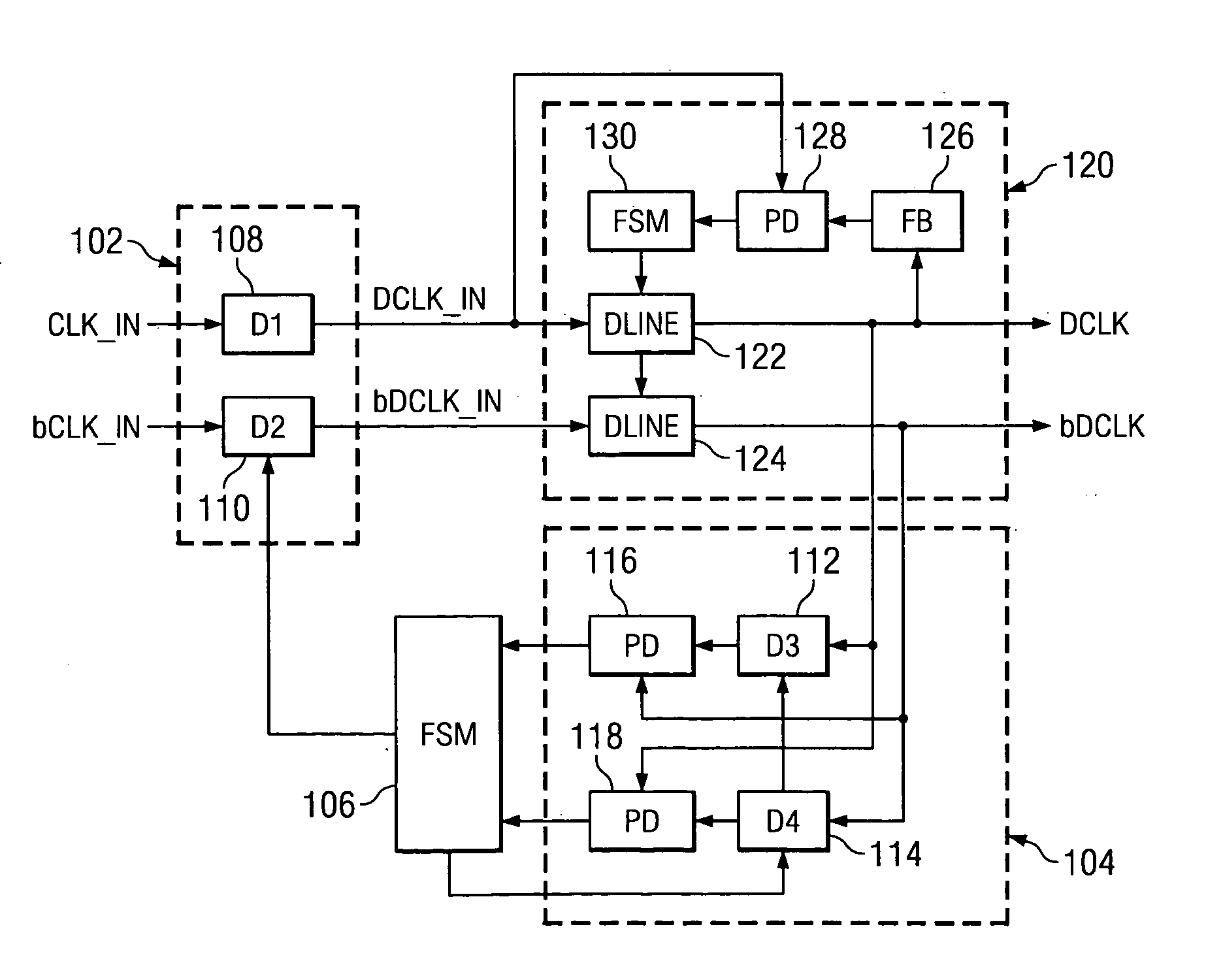
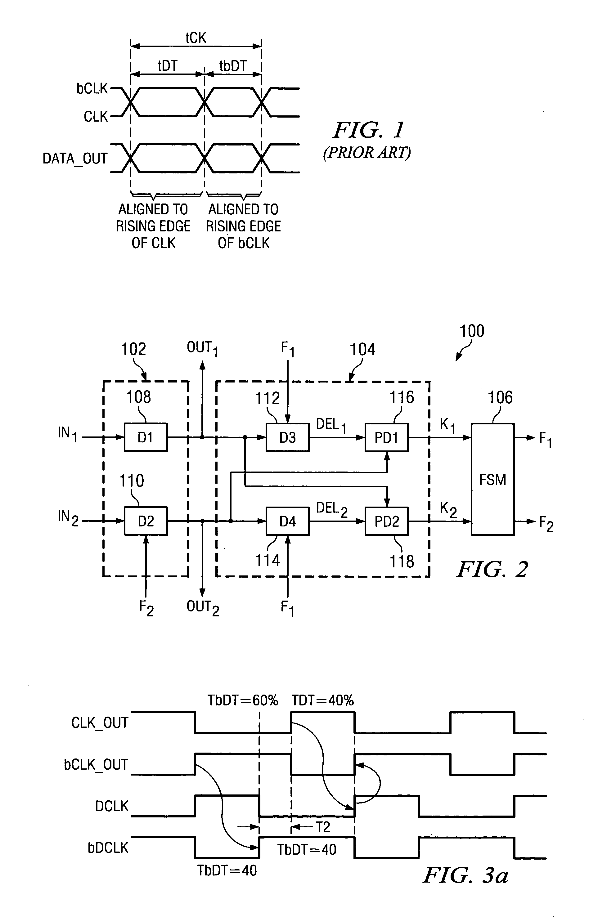
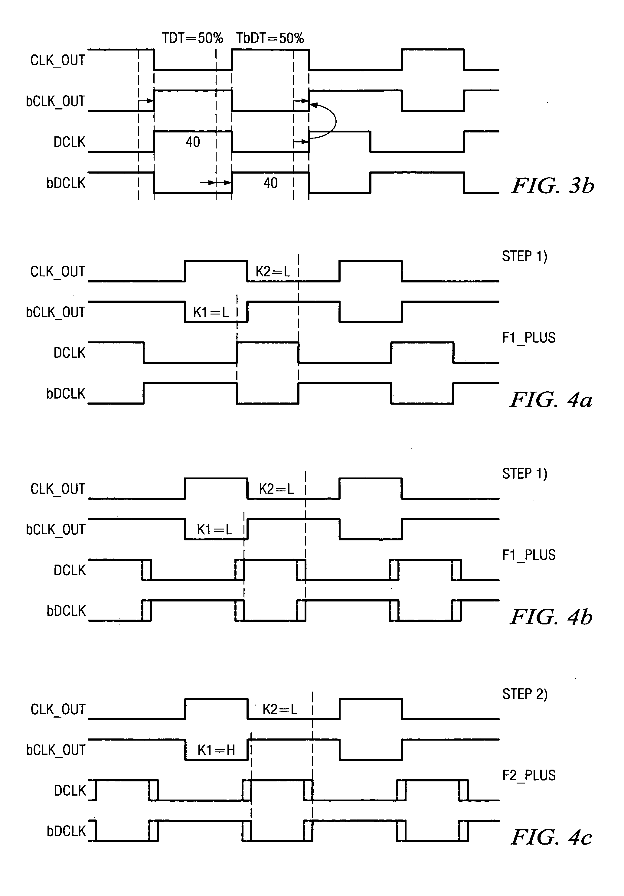
[0022] The present invention will be described with respect to preferred embodiments in a specific context, namely a differential clock of a double data rate (DDR) synchronous dynamic random access memory (DRAM). The invention may also be applied, however, to other systems that include complementary signals (either clocks or other signals) that desire to have the edge of one signal spaced a predetermined amount from the edge of the other signal. Examples include other memory devices as well as logic chips such as processors and communications chips.

[0023]FIG. 2 shows a blo...


PUM


Abstract

A method for adjusting the relative phases of two signals includes receiving first and second signals, which may, for example, be derived from a differential clock signal. A duty cycle error between the first signal and the second signal is detected by comparing a phase component of the first signal with a phase component of the second signal. This duty cycle error can then be corrected by delaying the second signal by an amount based upon a result derived from the comparing.

Description

TECHNICAL FIELD [0001] The present invention relates generally to electronic circuits, and more particularly to a system and method for a digital duty cycle corrector. BACKGROUND [0002] Semiconductors are generally used in integrated circuits for a wide range of electronic applications, including radios, televisions, cell phones, and personal computing devices, as examples. Over the years of development of integrated circuits, the structures used to form the integrated circuit elements such as transistors and diodes have been continually reduced in size to enable production of ever more complex devices in small sizes, with improved performance, and with low cost. An example of a highly integrated semiconductor device is a dynamic random access memory (DRAM) device in which a large number of transistors are configured to store a substantial amount of digital information in a very compact size with relatively low cost. [0003] One type of DRAM is a double data rate (DDR) synchronous dy...

Claims


Application Information

Patent Timeline
IPC IPC(8): H03L7/00
CPCH03K5/1565H03L7/0814H03L7/0805H03L7/07H03L7/0816
Inventor KIM, JOONHOKIM, JUNG PILLMINZONI, ALESSANDRO
Owner POLARIS INNOVATIONS
Why Eureka
Try Eureka