Method for fabricating an electronic component embedded substrate

a technology of embedded substrates and electronic components, which is applied in the manufacture of printed circuits, basic electric elements, solid-state devices, etc., can solve the problems of becoming difficult to form a wiring pattern with a sufficiently narrow pitch, the use of conventional printed circuit boards as substrates for mounting semiconductor elements is becoming less suitable, and it is difficult to fabricate electronic components having a thickness of 50 m, etc., to achieve the effect of easy and inexpensive embedded

Inactive Publication Date: 2006-01-05
SHINKO ELECTRIC IND CO LTD
View PDF12 Cites 102 Cited by
  • Summary
  • Abstract
  • Description
  • Claims
  • Application Information

AI Technical Summary

Benefits of technology

[0011] The present invention has been conceived in response to one or more of the problems of the related art, and its object is to provide a method for fabricating an electronic componen

Problems solved by technology

In turn, it is becoming difficult to form a wiring pattern with a sufficiently narrow pitch, corresponding to the pitch of electrode pads formed at the semiconductor element, on a conventional printed circuit board.
Therefore, use of the conventional printed circuit board as a substrate for mounting a semiconductor

Method used


Image

  • Method for fabricating an electronic component embedded substrate
  • Method for fabricating an electronic component embedded substrate
  • Method for fabricating an electronic component embedded substrate

Examples


first embodiment

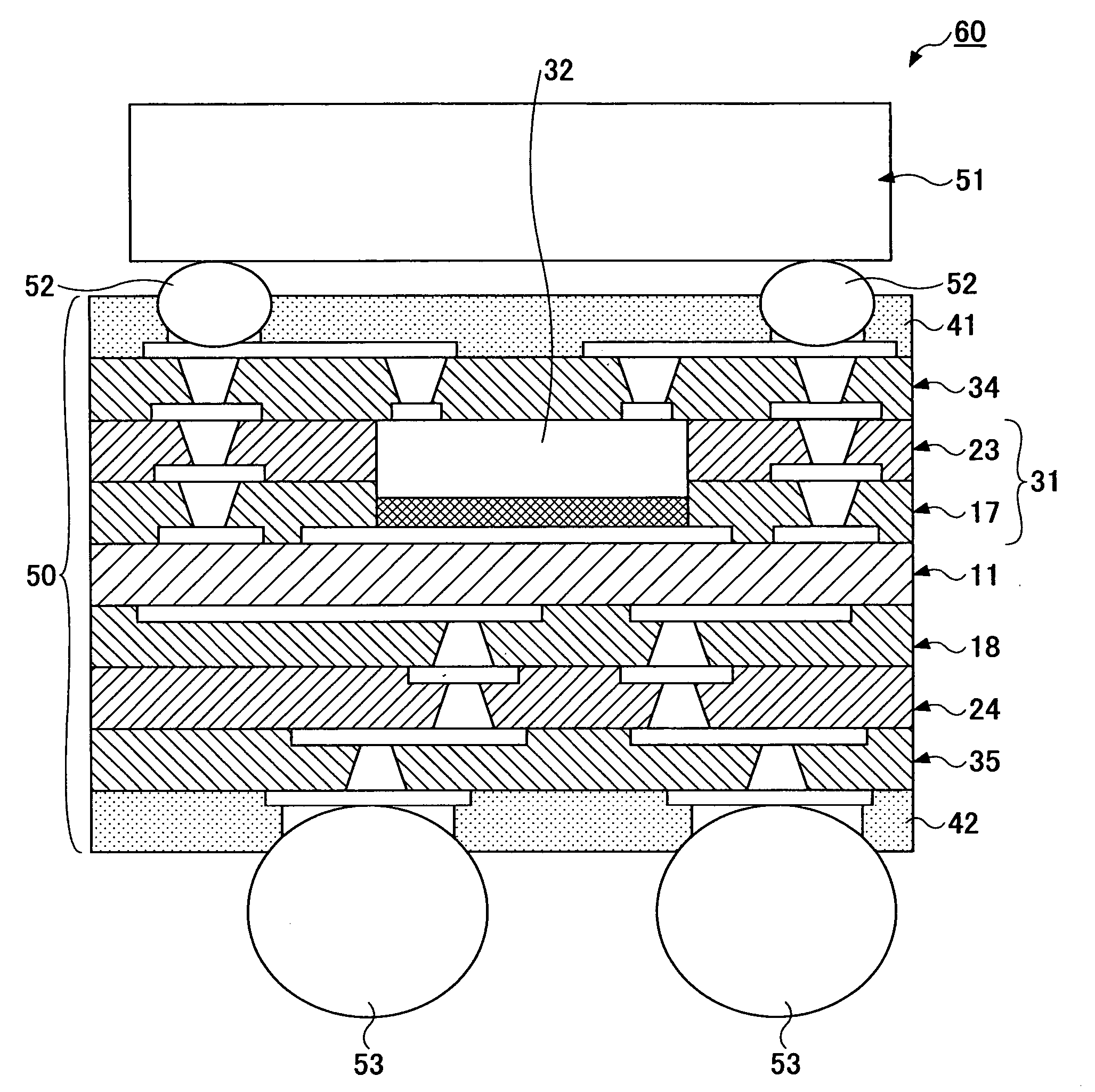
[0056] FIGS. 1˜10 are diagrams illustrating process steps of a method of fabricating an electronic component embedded substrate according to the present invention. Particularly, FIG. 9 is a diagram illustrating an electronic component embedded substrate 50 that is fabricated according to the fabrication method of the present embodiment, and FIG. 10 is a diagram illustrating a semiconductor device 60 that implements the electronic component embedded substrate 50. In the following, configurations of the electronic component embedded substrate 50 and the semiconductor device 60 that are fabricated according to the fabrication method of the present embodiment are described.

[0057] As is shown in FIG. 9, the electronic component embedded substrate 50 includes a core substrate 11, buildup layers 17, 18, 23, 24, 34, 35, an embedded electronic component 32, and solder resists 41 and 42, for example. The core substrate 11 may be formed by processing a double-sided copper clad laminate in a ma...

second embodiment

[0090] First, the method of fabricating the electronic component embedded substrate 50 is described with reference to FIGS. 11˜18.

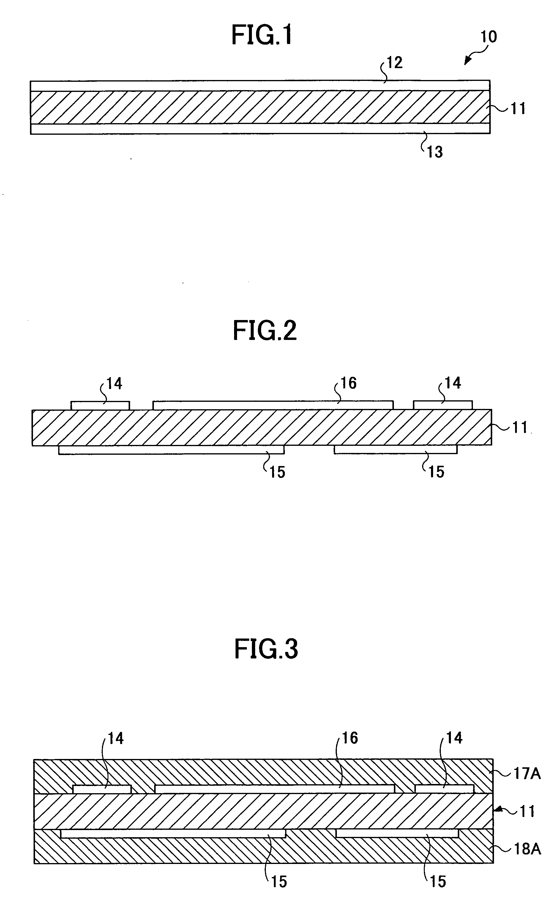
[0091] As is shown in FIG. 11, a copper clad laminate 10 is provided, and wirings 14, 15, and a stopper layer 16 are formed on a core substrate 11 in a manner similar to that described in relation to the first embodiment as is shown in FIG. 12. Then, insulating layers 17A and 18A are formed on the surfaces of the core substrate 11 having the wirings 14, 15 and the stopper layer 16 formed thereon as is shown in FIG. 13. It is noted that the process steps illustrated by FIGS. 11˜13 are identical to those illustrated by FIGS. 1˜3.

[0092] According to the present embodiment, a metal mask 61 is provided on the insulating layer 17A that is formed in the manner described above. The metal mask 61 may be made of copper or gold, for example, and includes an opening pattern 62 having a shape corresponding to the shape of a cavity 30 to be formed. FIG. 14 is a diagr...

third embodiment

[0105] In the following, the method of forming the electronic component embedded substrate 50 is described with reference to FIGS. 19˜22.

[0106] According to the present embodiment, a copper clad laminate 10 is provided as is shown in FIG. 19. The copper clad laminate 10 used in the present embodiment includes positioning pins 65 that are provided at predetermined positions. In the illustrated embodiment, the positioning pins 65 are provided at the periphery of the formation position of the electronic component embedded substrate 50. It is noted that the height of the positioning pins 65 is arranged to be greater than the thickness of the embedded electronic component 32.

[0107] Then, patterning is conducted on copper films 12 and 13 of the copper clad laminate 10 in a manner similar to that described in relation to the first embodiment so that wirings 14 and 15 are formed as is shown in FIG. 20. It is noted that in the present embodiment, a stopper layer 16 is not formed.

[0108] Th...


PUM


Abstract

A method for fabricating an electronic component embedded substrate including an electronic component that is embedded within a buildup layer is disclosed. The method includes a first buildup layer lamination step of laminating plural first buildup layers on a core substrate such that the total thickness of the first buildup layers corresponds to the thickness of the electronic component; a cavity formation step of forming a cavity for accommodating the electronic component at the laminated first buildup layers; an accommodating step of accommodating the electronic component within the cavity; and a second buildup layer lamination step of laminating a second buildup layer on the first buildup layers and the electronic component.

Description

BACKGROUND OF THE INVENTION [0001] 1. Field of the Invention [0002] The present invention relates to a method for fabricating an electronic component embedded substrate that includes an electronic component embedded within a multilayered circuit board. [0003] 2. Description of the Related Art [0004] In recent years and continuing, the operating frequency of semiconductor elements mounted on semiconductor devices is rising, and in turn, measures are being demanded for stabilizing the source voltage supplied to the semiconductor element. In response to such a demand, an electronic component embedded substrate has been proposed that includes an electronic component (e.g., capacitor element) that is embedded within a semiconductor device substrate on which a semiconductor element is mounted. [0005] Also, with the high densification of the semiconductor element, the pitch at which electrode pads are formed at the semiconductor element is becoming narrower. In turn, it is becoming difficu...

Claims


Application Information

Patent Timeline
IPC IPC(8): H01L21/44
CPCH01L21/4857H01L2224/16235H01L23/50H01L23/5389H01L24/24H01L24/82H01L25/0657H01L2224/16H01L2224/24226H01L2224/73267H01L2224/92H01L2224/92244H01L2924/01011H01L2924/01029H01L2924/01078H01L2924/01079H01L2924/15153H01L2924/1517H01L2924/15311H01L2924/19041H05K1/185H05K3/4644H01L23/49822H01L2224/0401H01L2225/1035H01L2224/32225H01L2224/04105H01L2924/014H01L2924/01033H01L2924/01006H01L2224/83H01L2224/82H01L2924/00H05K3/46
Inventor SUNOHARA, MASAHIROUEDA, KEISUKE
Owner SHINKO ELECTRIC IND CO LTD
Why Eureka
Try Eureka