Electrical circuit, thin film transistor, method for manufacturing electric circuit and method for manufactturing thin film transistor

a technology of thin film transistors and electric circuits, which is applied in the direction of dielectric characteristics, conductive pattern formation, thermoelectric devices, etc., can solve the problems of increasing the number of work steps, difficult to uniformly place ink at a desired position on the substrate, and not being suitable for manufacturing a complicated circuit pattern, etc., to achieve fine and complex circuit patterns, and simple and quick forming of electrical patterns

Inactive Publication Date: 2006-01-12
FLEX DISPLAY SOLUTIONS LLC
View PDF13 Cites 32 Cited by
  • Summary
  • Abstract
  • Description
  • Claims
  • Application Information

AI Technical Summary

Benefits of technology

[0010] In view of the foregoing problems, the present invention was achieved. An object of the present invention is to provide an electrical circuit as well as a thin film transistor capable of being simply and quickly formed without a thermal treatment, a method for simply and quickly forming an electrical circuit having a fine and complex circuit pattern, and a method for producing a thin film transistor.

Problems solved by technology

Namely, it has been difficult to uniformly place an ink at a desired position on the substrate.
However, the above technique also has a problem in that the solute of the ink is not impregnated in the adsorbing layer resulting in forming an accumulation of patterning materials on the surface of the adsorbing layer, which is not suitable for manufacturing a complicated circuit pattern, for example, a three-dimensional circuit pattern.
However, this method not only increases the number of work steps but also makes it difficult to use a polymer support which is suitably used for a flexible print circuit, as well as a flexible display.
However, in this method, there have been a disadvantage that it takes time until the solution is dried and pattern formation is completed.
In addition, patterning accuracy degrades due to spreading of liquid droplets.
Further, since a polyimide film is employed to form a channel via photolithography, complicated process are required, resulting in further increase in the production cost.

Method used


Image

  • Electrical circuit, thin film transistor, method for manufacturing electric circuit and method for manufactturing thin film transistor
  • Electrical circuit, thin film transistor, method for manufacturing electric circuit and method for manufactturing thin film transistor
  • Electrical circuit, thin film transistor, method for manufacturing electric circuit and method for manufactturing thin film transistor

Examples


example 1

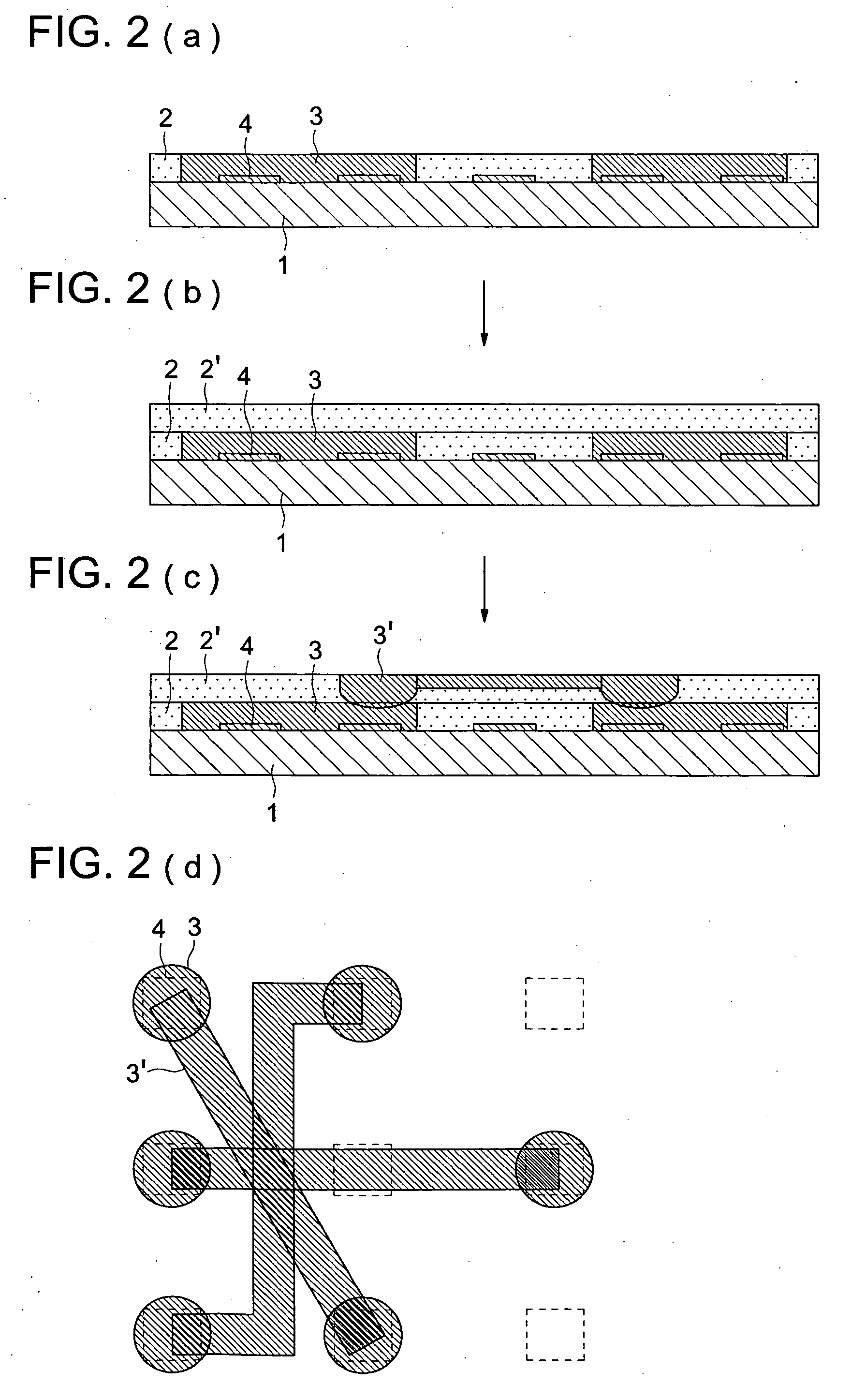
[0222] On substrate 1 which was a 200 μm thick PES film, a 200 nm thick aluminum film was deposited employing a sputtering method. Subsequently, the aluminum film was patterned by employing photolithography to form gate electrode 5 (refer to FIG. 4(a)). Further, a 200 nm thick silicon oxide film was formed under the following conditions, employing an atmospheric pressure plasma method to form gate insulator layer 6 (refer to FIG. 4(b)). The film temperature during the formation was maintained at 180° C.

(Used Gas)

[0223] Inert gas: helium 98.25 percent by volume

[0224] Reactive gas: oxygen gas 1.5 percent by volume

[0225] Reactive gas: tetraethoxysilane vapor (bubbled employing helium gas) 0.25 percent by volume

(Discharge Condition)

[0226] Discharge power: 10 W / cm2

[0227] Further, water repellent treatment was performed on a silicon oxide film, employing a plasma method.

[0228] Further, on gate insulation layer 6, pentacene, as semiconductor 4a, was formed with a thickness of 50 ...

example 2

[0234] A thin film transistor was prepared in the same manner as Example 1, except that a 5 μm thick polyvinyl alcohol (PVA) layer was formed as a receptive layer by employing an aqueous PVA solution. The mobility of carriers in the saturated region was 0.08 cm2 / Vs.


PUM

PropertyMeasurementUnit
electrical conductivityaaaaaaaaaa
particle diameteraaaaaaaaaa

Abstract

An electrical circuit containing a substrate having thereon a receptive layer, wherein the receptive layer has a conductive polymer impregnated in the receptive layer, and a method for forming the electrical circuit.

Description

TECHNICAL FIELD [0001] The present invention relates to an electrical circuit and a production method of the same, as well as a thin film transistor and a production method of the same. BACKGROUND OF THE INVENTION [0002] Common methods for forming electrical circuit patterns on a substrate are such that after forming, on the entire surface of the substrate, a conductive film, an insulating film, a semiconductor film, and a dielectric film, employing vacuum processes such as sputtering, circuit patterning is performed employing photolithographic techniques. Photolithographic techniques, as described herein, refer to the method in which a photosensitive resist is applied onto the thin film to be subjected to patterning, and after being exposed via a photomask and developed, thin exposed film portions are subjected to dry etching or wet etching. Thereafter, commonly, the resist is peeled off and after forming a film of another material, the photolithographic process is repeated. [0003]...

Claims


Application Information

Patent Timeline
Patent Type & Authority Applications(United States)
IPC IPC(8): H01L29/08H01L21/288H01L21/3205H01L21/336H01L21/58H01L29/786H01L51/00H01L51/30H01L51/40H05K3/12H05K3/46
CPCH01L51/002H01L51/0021H01L51/0035H01L51/0036H01L51/0038H05K2201/0329H01L51/0512H05K3/125H05K3/4644H05K2201/0116H01L51/0508H10K71/60H10K71/30H10K85/111H10K85/113H10K85/114H10K10/46H10K10/462
Inventor HIRAI, KATSURA
Owner FLEX DISPLAY SOLUTIONS LLC
Why Eureka
Try Eureka