Extreme low-K interconnect structure and method

a technology of interconnects and low-k, applied in the direction of semiconductor devices, semiconductor/solid-state device details, electrical apparatus, etc., can solve the problems of improved ic performance, rc delay problems, printed circuit boards, pcb's, etc., and achieve critical mechanical strength reduction for each film

Inactive Publication Date: 2006-01-12
LSI CORPORATION
View PDF25 Cites 183 Cited by
  • Summary
  • Abstract
  • Description
  • Claims
  • Application Information

AI Technical Summary

Benefits of technology

[0004] In accordance with the principles of the present invention, improved methods and st

Problems solved by technology

As integrated circuit (IC) design continues to evolve, one of the important barriers to improved IC performance is RC time delay.
Although these problems are particularly evident in smaller circuit structures, such as IC's, they are also present in many other types of electrical circuit structures.
Such RC delay problems are also experienced in printed circuit boards (PCB's).
However, each of these films suffers from critical reductions in mechanical st

Method used


Image

  • Extreme low-K interconnect structure and method
  • Extreme low-K interconnect structure and method
  • Extreme low-K interconnect structure and method

Examples


Embodiment Construction

[0014] The present invention has been particularly shown and described with respect to certain embodiments and specific features thereof. The embodiments set forth hereinbelow are to be taken as illustrative rather than limiting. It should be readily apparent to those of ordinary skill in the art that various changes and modifications in form and detail may be made without departing from the spirit and scope of the invention.

[0015] In the following detailed description, fabrication methods and apparatus for constructing electrical conduction structures demonstrating extreme low-K properties will be disclosed.

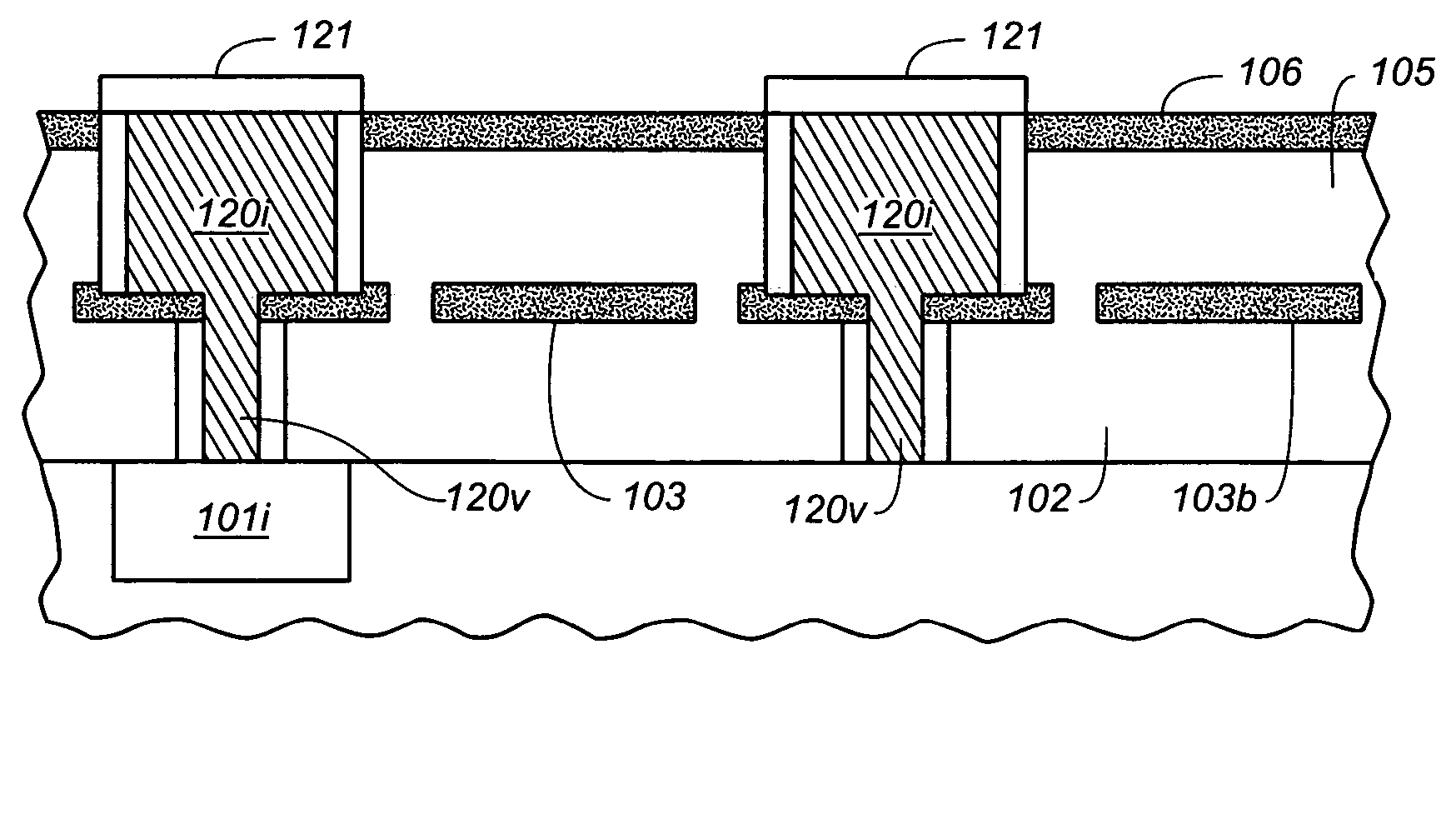
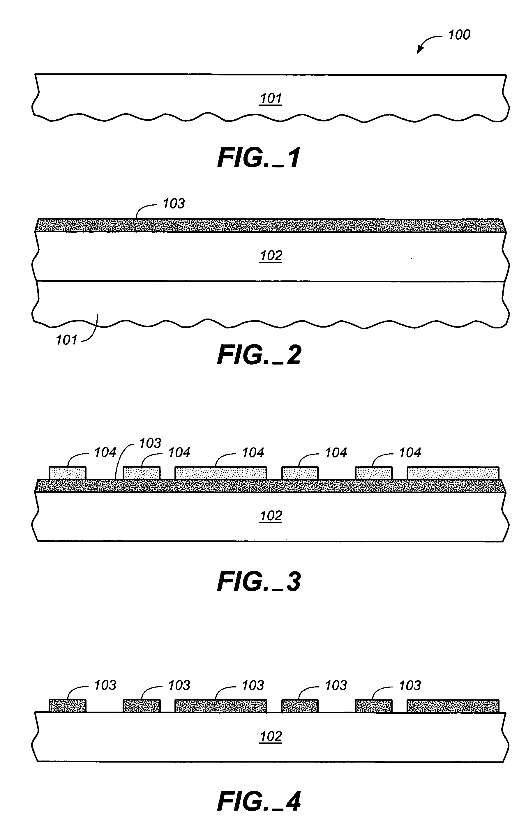
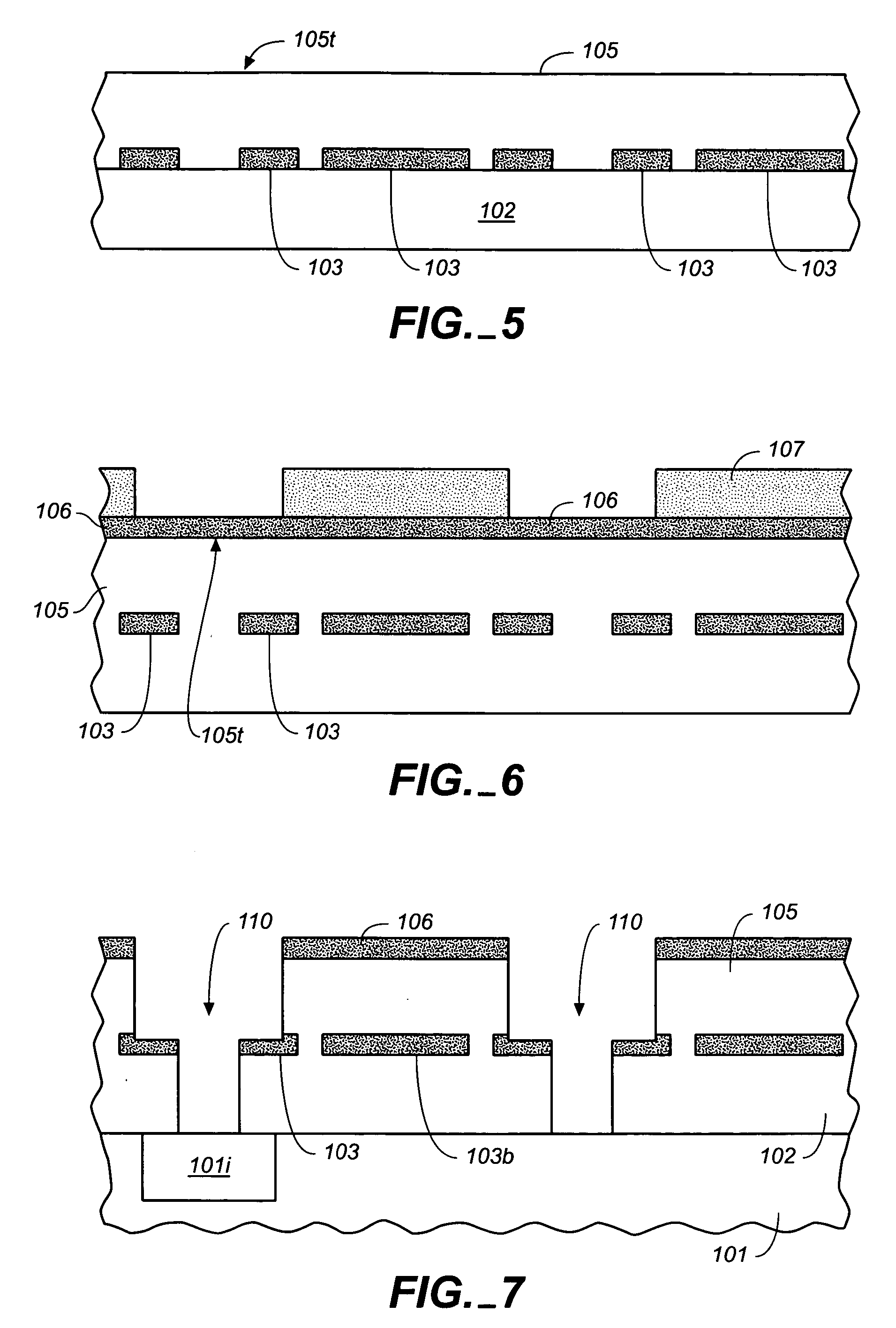
[0016]FIG. 1 is a simplified schematic depiction of a substrate structure 100 in the process of fabrication in accordance with an embodiment of the invention. In one depicted embodiment, a top portion of a substrate 101 suitable for implementation in accordance with the principles of the invention is shown. The inventors point out that the principles of the invention can be ap...


PUM


Abstract

Embodiments of the invention include an extreme low-K circuit structure formed on a substrate having a plurality of electrically conductive structures. A lattice structure of bracing material configured to support the electrically conductive structures is formed on the substrate and also can define regions of extreme low-K dielectric space between the electrically conductive structures. Additionally, methods for creating dielectric structures on a substrate are disclosed.

Description

TECHNICAL FIELD [0001] The invention described herein relates generally to methods and structures used to form interconnect lines having high strength while still exhibiting extreme low-K dielectric properties between the interconnect lines. BACKGROUND [0002] As integrated circuit (IC) design continues to evolve, one of the important barriers to improved IC performance is RC time delay. Such delay is induced, in part, by capacitance that exists between the various levels of electrical interconnects in an IC die. Although these problems are particularly evident in smaller circuit structures, such as IC's, they are also present in many other types of electrical circuit structures. Such RC delay problems are also experienced in printed circuit boards (PCB's). Conventional solutions to this problem have been the increasing reliant on highly conductive (lower resistance) interconnect materials such as copper. Also, insulating materials having increasingly lower dielectric constants have ...

Claims


Application Information

Patent Timeline
IPC IPC(8): H01L23/48
CPCH01L21/3122H01L21/76807H01L21/7681H01L21/7682H01L21/76831H01L21/76844H01L2924/0002H01L23/49894H01L23/5329H01L23/53295H01L2924/00H01L21/76829H01L21/02164
Inventor ALLMAN, DERRYL D. J.MAY, CHARLES E.
Owner LSI CORPORATION
Why Eureka
Try Eureka