Contactless IC card system

a ic card and contactless technology, applied in the field of contactless ic card systems, can solve the problems of low power efficiency of conventional modulating circuits, complex circuit arrangement, and inability to meet the necessary items of ic card systems, and achieve the effect of simple and easy manufacturing and high efficiency

Inactive Publication Date: 2006-01-12
SONY CORP
View PDF4 Cites 8 Cited by
  • Summary
  • Abstract
  • Description
  • Claims
  • Application Information

AI Technical Summary

Benefits of technology

[0018] The present invention has been made to solve the above-explained drawbacks of the prior art, and therefore, has an object to provide a modulating circuit, a demodulating circuit, an amplifying circuit used in this modulating circuit, and furthermore, a transmitter apparatus as well as a receiver apparatus with employment of these modulating circuit and demodulating circuit, which can be simply and easily manufactured with an IC form in combination with other circuit blocks, and also which can be operated in high efficiencies.
[0019] Another object of the present invention is to provide the following modulating circuit, amplifying circuit applicable to this modulating circuit, and also a transmitter apparatus with using this modulating circuit. That is, first and second output signals having predetermined phases with respect to an input signal are added to each other, and the added result is outputted. At least, the second output signal is gated in response to the input data. Also, on the output side of a power amplifying circuit, the power-amplified results are attenuated in accordance with the input data so as to produce an amplitude-modulated signal. This circuit arrangement can be simply and readily manufactured in the IC form together with other circuit blocks.
[0020] Also, since amplitude-modulated signals are biased to be amplified, or clamped, a demodulating circuit and a receiver apparatus with using this demodulating circuit can be simply and easily manufactured in the IC form in combination with other circuit blocks.
[0021] Furthermore, amplitude-modulated signals are clamped, polarities of these amplitude-modulated signals are judged to multiply the polarity judgment result by the amplitude-modulated signals, and furthermore, the amplitude-modulated signals are selectively outputted based upon the polarity judgment results of the amplitude-modulated signals. As a result, another demodulating circuit and another receiver apparatus with using this demodulating circuit can be simply and readily manufactured in the IC form together with other circuit blocks.

Problems solved by technology

Moreover, these modulating circuits and demodulating circuits with employment of the conventional circuit arrangements can hardly satisfy the necessary items for the IC card systems.
This voltage range limitation causes the lower power efficiency of the conventional modulating circuit.
Also, as to the modulating circuit with employment of the multiplying circuit, there are such drawbacks that the circuit arrangement becomes complex, and this complex modulating circuit cannot be simply and readily manufactured in the IC form.
Also, this power amplifying circuit has a drawback in that in order to transmit sufficiently high power, the active elements capable of satisfying the necessary allowable current and the allowable loss must be used instead of commercially available general-purpose electronic components.
In contrast, the demodulating circuit arranged by the envelope detecting circuit with employment of the diode owns such a drawback that a leakage current is produced in the diode when this demodulating circuit is manufactured in the IC form, and therefore, the detection efficiency of the ASK modulation signal is considerably lowered.
On the other hand, in the conventional demodulating circuit arranged by the synchronization detecting circuit, there is another drawback in that the circuit arrangement of the phase synchronization system circuit 9 becomes complex.

Method used


Image

  • Contactless IC card system
  • Contactless IC card system
  • Contactless IC card system

Examples


first embodiment

Advantages of First Embodiment

[0278] In accordance with the above-described circuit arrangement of the first embodiment, with respect to the power-amplified output of the power amplifying circuit 59 for power-amplifying the carrier signal SC by a predetermined phase, the power-amplified output of the power amplifying circuit 59 for similarly power-amplifying the carrier signal SC by a preselected phase is gated to be added in response to the logic level of the transmit data stream “D(R→C)”. As a consequence, the power-amplified ASK modulation signal can be produced by employing the power amplifying circuits which are designed by mainly considering the power efficiency without considering the linearity thereof to some extent. Therefore, the power efficiencies of these power amplifying circuit can be increased, as compared with those of the conventional power amplifying circuits. Also, these power amplifying circuits may be constituted by employing the commercially available electroni...

second embodiment

ASK Modulating Circuit of Second Embodiment

[0280] As shown in FIG. 15 in contrast with FIG. 9, there is indicated a basic idea of an ASK modulating circuit applied to a second embodiment of the present invention. In this ASK modulating circuit 79, the power-amplified results obtained from the power amplifying circuits 59 and 62 are supplied to two signal paths of antennas 28A and 28B, respectively. These two power-amplified results are added to each other in electromagnetic fields transmitted from the antennas 28A and 28B.

[0281] As represented in FIG. 15, even when the ASK modulating circuit is so arranged that these two power-amplified results are added to each other in the electromagnetic fields, it is possible to achieve a similar effect to that of the first embodiment.

third embodiment

ASK Modulating Circuit of Third Embodiment

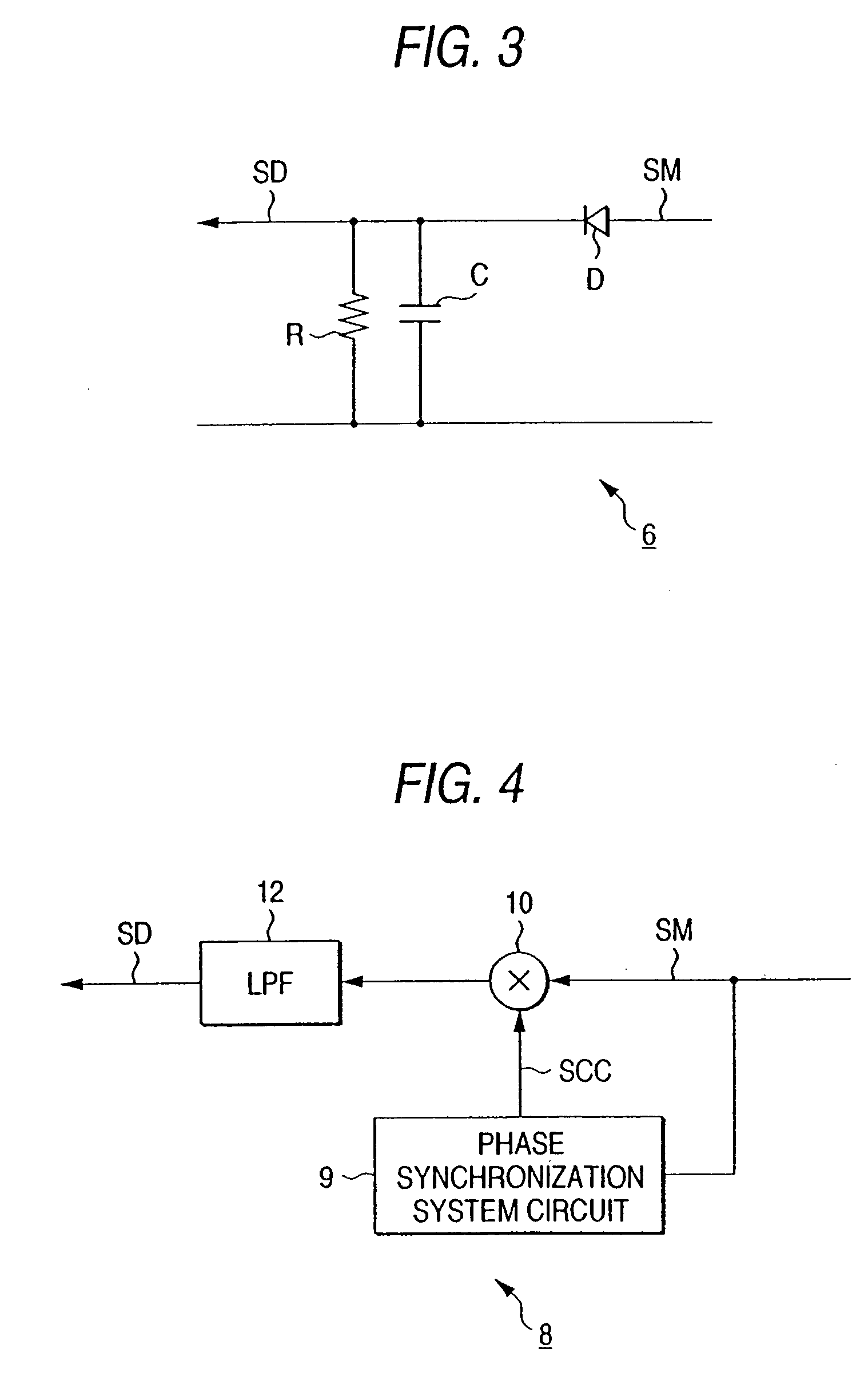
[0282]FIG. 16 is a block diagram for representing a basic arrangement of an ASK modulating circuit applied to a third embodiment of the present invention. In this third embodiment, this ASK modulating circuit 80 is applied instead of the ASK modulating circuit 47 and the power amplifying circuit 48 (see FIG. 8) of the reader / writer 23.

[0283] In other words, in the ASK modulating circuit 80, after the carrier signal is amplified by the power amplifying circuit 81, the amplified carrier signal is outputted via a variable attenuator 82. In response to the transmit data stream TX(D(R→C)), the variable attenuator 82 attenuates this carrier signal to thereby output the attenuated carrier signal. As a result, this ASK modulating circuit 80 outputs such an ASK modulation signal SM, the amplitude of which is varied in response to the transmit data stream TX(D(R→C)).

[0284] As a typical variable attenuator type, for example, the variable attenuator 8...


PUM


Abstract

In a contactless IC card system, a modulating circuit manufactured in an IC form is operable at a high power efficiency. The demodulating apparatus is configured to include: first signal output means for outputting a first output signal having a predetermined phase with respect to that of an input signal, a second signal output means for outputting a second output signal having a predetermined phase with respect to that of the input signal, gate means for gating at least the second output signal, calculation means for adding, or subtracting the first output signal and the second output signal; and control means for controlling the operation of the gate means in response to a logic level of input data.

Description

[0001] This is a divisional of application Ser. No. 10 / 442,736, filed May 21, 2003, which is a divisional of application Ser. No. 09 / 751,140, filed Dec. 29, 2000, which is a divisional of application Ser. No. 09 / 327,757, filed Jun. 7, 1999 and issued as U.S. Pat. No. 6,198,361 on Mar. 6, 2001.BACKGROUND OF THE INVENTION [0002] The present invention generally relates to a contactless IC card system. More specifically, the present invention is directed to an amplifying circuit, a modulating circuit, a demodulating circuit, a transmitter apparatus, and a receiver apparatus, applicable to a contactless IC card capable of reading / writing various sorts of data in a contactless manner, and is also applicable to an IC card reader / writer capable of communicating data with this contactless IC card. [0003] Conventionally, in IC card systems which employ IC cards, these IC card systems are applied to ticket inspection systems used in transportation facilities, and person entrance / exit managemen...

Claims


Application Information

Patent Timeline
Patent Type & Authority Applications(United States)
IPC IPC(8): H03C1/00G06K17/00G06K19/07H03F3/72H03K7/02H04B1/59H04L27/04H04L27/06
CPCG06K7/0008G06K19/0723H03C1/08H03C1/14H03C1/36H04L27/06H03F2200/327H03F2203/7215H03K7/02H04L27/04H03F3/72
Inventor ARISAWA, SHIGERU
Owner SONY CORP
Why Eureka
Try Eureka