Super lattice tunnel junctions

Inactive Publication Date: 2006-01-19
II VI DELAWARE INC
View PDF2 Cites 27 Cited by
  • Summary
  • Abstract
  • Description
  • Claims
  • Application Information

AI Technical Summary

Benefits of technology

[0012] The present invention relates to using a super lattice structure in conjunction with a tunnel junction to provide an improved contact for multiple components. A tunnel junction for providing a common connection to two components is described. The tunnel junction can include a first semiconductor material having a resistance parameter for conducting a current and a second semiconductor material having a resistance parameter that is more restrictive to conduction of a current than the resistance parameter of the first semiconductor material. The first semiconductor material can have a critical thickness at which lattice matching of the first semiconductor material causes dislocation. The second semiconductor material can have a critical thickness at which lattice matching of the second semiconductor material causes dislocation, wherein the critical thickness of the second semiconductor is thicker than the critical thickness of the first semiconductor material.
[0013] An optoelectronic device is described. The optoelectronic device can include a vertical cavity surface emitting laser (VCSEL) diode, a tunnel junction and a photodiode. The VCSEL can include a first PN junction with a first p layer and a first n layer. The tunnel junction can be coupled monolithically to the VCSEL diode. The tun

Problems solved by technology

In some instances a tunnel junction made from a combination of III-V semiconductor materials would have the desired resistance properties, but it has not been possible to use this combination of III-V semiconductor materials for various reasons.
One reason why a combination of III-V semiconductor material cannot be used is because the III-V semiconductor materials have a mismatched lattice parameter resulting in a critical thickness that is too thin to be used without the tunnel junction experiencing a dislocation and subsequent cracking.
Two constraints, however, that limit the relative proportion of In to Ga and As are the necessary thickness of a tunnel junction and the critical thickness of

Method used


Image

  • Super lattice tunnel junctions
  • Super lattice tunnel junctions
  • Super lattice tunnel junctions

Examples


Embodiment Construction

[0030] The present invention is related to improved tunnel junctions. The principles of the present invention are described with reference to the attached drawings to illustrate the structure and operation of example embodiments used to implement the present invention. Using the diagrams and description in this manner to present the invention should not be construed as limiting its scope. Additional features and advantages of the invention will in part be obvious from the description, including the claims, or may be learned by the practice of the invention. Descriptions of well-known components and processing techniques are omitted so as not to unnecessarily obscure the invention in detail.

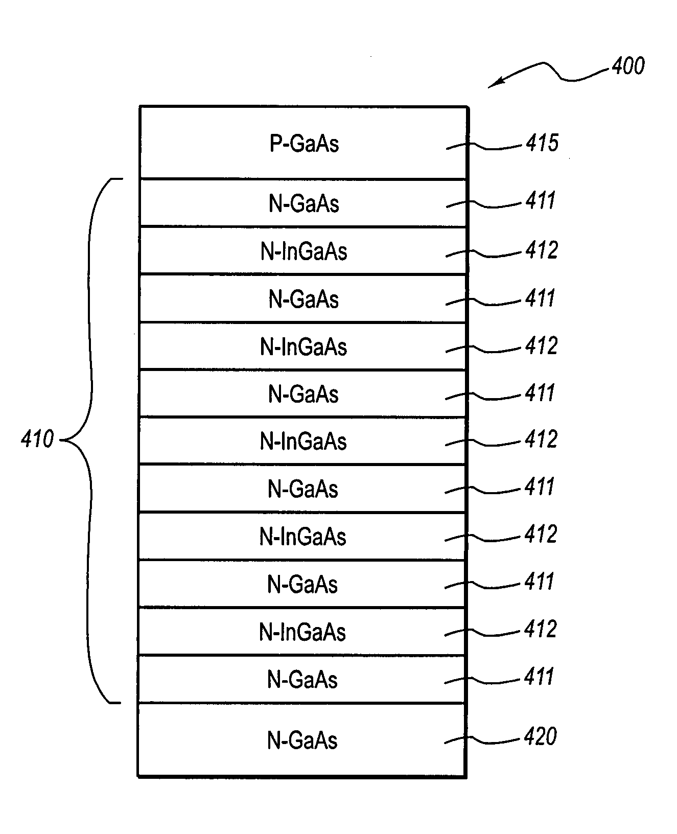
[0031] Embodiments of the present invention include devices incorporating super lattice tunnel junctions. For example, several example embodiments of the present invention include monolithically formed laser diodes and photodiodes where a common contact is provided by an improved tunnel junction....


PUM


Abstract

Super lattice structures in conjunction with a tunnel junction to provide an improved contact for multiple components. The tunnel junctions can include a first semiconductor material having a resistance parameter for conducting a current and a second semiconductor material having a resistance parameter that is more restrictive to conduction of a current than the resistance parameter of the first semiconductor material. The first semiconductor material can have a critical thickness at which lattice matching of the first semiconductor material causes dislocation. The second semiconductor material can have a critical thickness at which lattice matching of the second semiconductor material causes dislocation that is thicker than the critical thickness of the first semiconductor material. The tunnel junction can be used in a monolithically manufactured photo transmitter and receiver design.

Description

CROSS-REFERENCE TO RELATED APPLICATIONS [0001] This application is a continuation in part of U.S. patent application Ser. No. 10 / 877,915 entitled “Light Emitting Device With an Integrated Monitor Photodiode” filed Jun. 25, 2004, the contents of which is hereby expressly incorporated by reference herein.BACKGROUND OF THE INVENTION [0002] 1. The Field of the Invention [0003] The invention generally relates to tunnel junctions. More specifically, the invention relates to using a super lattice structure in conjunction with a tunnel junction to provide an improved contact for multiple components. [0004] 2. Description of the Related Art [0005] Tunnel junctions are used in various applications to provide a common connection between two components. One application of tunnel junctions is in the design of components made at least in part from III-V (three-five) semiconductor materials. In such applications it can be advantageous to have a low resistance tunnel junction. Often, in order to ob...

Claims


Application Information

Patent Timeline
IPC IPC(8): H01L29/24H01S5/00H01S5/026H01S5/183
CPCH01S5/0264H01S5/18308H01S5/18313H01S5/1835H01S2301/02H01S5/2022H01S5/2027H01S5/3095H01S5/18358
Inventor DEBRAY, JEAN-PHILIPPE MICHELGUENTER, JAMES K.
Owner II VI DELAWARE INC
Why Eureka
Try Eureka